
CAN Board - Datasheet
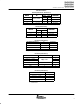
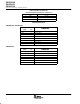
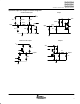
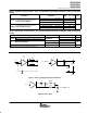
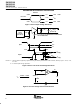
Table Of Contents
- FEATURES
- APPLICATIONS
- DESCRIPTION
- Function Tables
- Terminal Functions
- equivalent input and output schematic diagrams
- absolute maximum ratings over operating free-air temperature (see Note \ 1) (unless otherwise noted) †
- recommended operating conditions
- ELECTRICAL SPECIFICATIONS
- driver electrical characteristics over recommended operating conditions \ (unless otherwise noted)
- driver switching characteristics over recommended operating conditions(\ unless otherwise noted)
- receiver electrical characteristics over recommended operating condition\ s (unless otherwise noted)
- receiver switching characteristics over recommended operating conditions\ (unless otherwise noted)
- device switching characteristics over recommended operating conditions (\ unless otherwise noted)
- device control-pin characteristics over recommended operating conditions\ (unless otherwise noted)
- PARAMETER MEASUREMENT INFORMATION
- TYPICAL CHARACTERISTICS
- APPLICATION INFORMATION
- MECHANICAL DATA
- IMPORTANT NOTICE

SN65HVD230
SN65HVD231
SN65HVD232
SLOS346G – MARCH 2001 – REVISED JUNE 2002
7
www.ti.com
driver electrical characteristics over recommended operating conditions (unless otherwise noted)
PARAMETER TEST CONDITIONS MIN TYP
†
MAX UNIT
V
Dominant
V
I
= 0 V
,
CANH 2.45 V
CC
V
OH
Bus output voltage
Dominant
V
I
=
0
V
,
See Figure 1 and Figure 3
CANL 0.5 1.25
V
V
Bus output voltage
Recessive
V
I
= 3 V
,
CANH 2.3
V
V
OL
Recessive
V
I
=
3
V
,
See Figure 1 and Figure 3
CANL 2.3
V
Dominant
V
I
= 0 V, See Figure 1 1.5 2 3
V
V
OD(D)
Differential output
Dominant
V
I
= 0 V, See Figure 2 1.2 2 3
V
V
Differential
out ut
voltage
Recessive
V
I
= 3 V, See Figure 1 –120 0 12 mV
V
OD(R)
Recessive
V
I
= 3 V, No load –0.5 –0.2 0.05 V
I
IH
High-level input current V
I
= 2 V –30 µA
I
IL
Low-level input current V
I
= 0.8 V –30 µA
I
Short circuit output current
V
CANH
= –2 V –250 250
mA
I
OS
Short-circuit output current
V
CANL
= 7 V
–250 250
mA
C
o
Output capacitance See receiver
Standby SN65HVD230 V
(Rs)
= V
CC
370 600
A
I
CC
Su
pp
ly current
Sleep SN65HVD231 V
(Rs)
= V
CC
, D at V
CC
0.04 1
µA
I
CC
Supply current
All devices
Dominant V
I
= 0 V, No load Dominant 10 17
mA
All devices
Recessive V
I
= V
CC
, No load Recessive 10 17
mA
†
All typical values are at 25°C and with a 3.3-V supply.
driver switching characteristics over recommended operating conditions(unless otherwise noted)
SN65HVD230 and SN65HVD231
PARAMETER
TEST
CONDITIONS
MIN TYP MAX UNIT
V
(Rs)
= 0 V 35 85
t
PLH
Propagation delay time, low-to-high-level output
R
S
with 10 kΩ to ground
70 125
ns
t
PLH
Pro agation
delay
time,
low to high level
out ut
R
S
with 100 kΩ to ground 500 870
ns
V
(Rs)
= 0 V 70 120
t
PHL
Propagation delay time, high-to-low-level output
R
S
with 10 kΩ to ground
130 180
ns
t
PHL
Pro agation
delay
time,
high to low level
out ut
R
S
with 100 kΩ to ground 870 1200
ns
V
(Rs)
= 0 V 35
t
sk
(
p
)
Pulse skew (|t
PHL
– t
PLH
|)
R
S
with 10 kΩ to ground
C
L
= 50 pF,
See Figure 4
60
ns
t
sk( )
Pulse
skew
(|t
PHL
t
PLH
|)
R
S
with 100 kΩ to ground
S
ee
Fi
gure
4
370
ns
t
r
Differential output signal rise time
V0V
25 50 100 ns
t
f
Differential output signal fall time
V
(Rs)
= 0 V
40 55 80 ns
t
r
Differential output signal rise time
R with 10 kΩ to ground
80 120 160 ns
t
f
Differential output signal fall time
R
S
with 10 kΩ to ground
80 125 150 ns
t
r
Differential output signal rise time
R with 100 kΩ to ground
600 800 1200 ns
t
f
Differential output signal fall time
R
S
with 100 kΩ to ground
600 825 1000 ns