
User's Manual


Wireless Cables Inc.
2880 Zanker Rd, Suite 203, San Jose, CA 95134
T 408.954.7301 ~ F 408.228.0687
sales@aircable.net ~ www.aircable.net
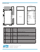
Terminal Description
1 PIO(10) I/O 3.3V TTL PIO(10), used for button input, weak pull-down resistor
2 LED(0) O Supply connected to PIO(2), used for EEPROM power control
3 WAKEUP I Supply Wakeup from deep sleep, connected to PIO(10)
4 VBATT I/O Supply 3V Coin cell, 3.3V supply or battery, positive terminal
5 AIO(0) I Analog Analog input or output 0-1.3V
6 AIO(1) I Analog Analog input or output 0-1.3V
7 SPI_RESET I 3.3V TTL High enables SPI interface for programming and debugging
8 SPI_MISO I 3.3V TTL SPI rmware programming, same as PIO(8)
9 SPI_CSB I 3.3V TTL SPI rmware programming, same as PIO(6)
10 SPI_CLK I 3.3V TTL SPI rmware programming, same as PIO(5)
11 SPI_MOSI O 3.3V TTL SPI rmware programming, same as PIO(7)
12 CTS connected to RTS for compatib ility
13 TX O 3.3V TTL Uart async serial output, same as PIO(0)
14 RTS shorted with CTS for compatibility
15 RX I 3.3V TTL Uart async serial input, same as PIO(1)
16 NC not connected
17 VIN I Supply Regulator input, 3V – 12V
18 GND Supply Ground
PIO(10)
LED_CHG
WAKEUP
VBATT
AIO(0)
AIO(1)
SPI_RESET
SPI_MISO (pio8)
SPI_CSB (pio6)
SPI_CLK (pio5)
SPI_MOSI( pio12)
TX (pio0)
RX (pio1)
1V35
VIN
GND
PIO(9)
GND
PIO(6)
PIO(8)
PIO(11)
PIO(7)
PIO(2)
PIO(3)
PIO(4)
PIO(5)
SCL
SDA
Pin Functions
Viewed from Component Side
GND
ANT
GND
AIO2
14.50mm
31.00mm
1.27mm
1.2mm
1
2
3
4
5
6
7
8
9
10
11
12
13
14
15
16
17
18
36
35
34
33
32
31
30
29
28
27
26
25
24
23
22
21
20
19
Optional Antenna Area
24.90mm
2.0mm
2.1mm
41 40 39 38
smd pad: 1mm x 0.5mm
PCB Layout