
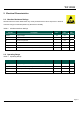
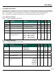
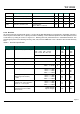
Specifications


Page 16
WT1231H
3. Module Description
This section describes in depth the architecture of the WT1231H low-power, highly integrated transceiver.
3.1. Power Supply Strategy
The WT1231H employs an advanced power s
upply scheme, which provides stable operating characteristics over the
full temperature and voltage range of operation. This includes the full output power of +20dBm maintained from 2.4 to 3.6V.
The WT1231H can be powered from any low-noise voltage source via pins VBAT1 and VBAT2. Decoupling
capacitors should be connected, as suggested in the reference design, on VR_PA, VR_DIG and VR_ANA pins to
ensure a correct operation of the built-in voltage regulators.
3.2. Frequency Synthesis
The LO generation on the WT1231H is based on a state-of-the-art fractional-N PLL. The PLL is fully integrated
with automatic calibration.
3.2.1. Reference Oscillator
The crystal oscillator is the main timing reference of the WT1231H. It is used as a reference for the frequency
synthesizer and as a clock for the digital processing.
The XO startup time, TS_OSC, depends on the actual XTAL being connected on pins XTA and XTB. When using the built-
in sequencer, the WT1231H optimizes the startup time and automatically triggers the PLL when the XO signal is stable.
To manually control the startup time, the user should either wait for TS_OSC max, or monitor the signal CLKOUT which
will only be made available on the output buffer when a stable XO oscillation is achieved.
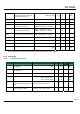
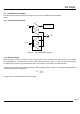
An e
x
ternal clock can be used to replace the crystal oscillator, for instance a tight tolerance TCXO. To do so, bit 4 at
address 0x59 should be set to 1, and the external clock has to be provided on XTA. XTB should be left open. The peak-
peak amplitude of the input signal must never exceed 2.4 V. Please consult your TCXO supplier for an appropriate value
of decoupling capacitor, C
D
.
XTA
XTB
TCXO
32
MHz
NC
OP
Vcc
Vcc
GND
C
D
Figure 4. TCXO
Connection