Wireless-Tag Technology Co., Ltd. V1.0.0 WT32C3-01N Datasheet V1.0.0 July 16, 2021 Wireless-Tag Technology Co., Ltd I Copyright ©2020 Wireless-Tag Technology Co., Ltd. All Rights Reserved. http://www.wireless-tag.
Wireless-Tag Technology Co., Ltd. V1.0.0 About this document This document provides users with the technical specifications for WT32C3-01N. Document updates Please visit Wireless-Tag’s official website to download the latest version of the document. Revision history Please go to the document revision history page to view the revisions of the document. Disclaimer and copyright notice Information in this paper, including URL references, is subject to change without prior notice.
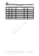
Wireless-Tag Technology Co., Ltd. V1.0.0 Revision History No. Version Changes Change (+/-) Descriptions Author Date 1 V1.0.0 C First release Fiona July 16, 2021 *Changes:C――create, A——add, M——modify, D——delete III Copyright ©2020 Wireless-Tag Technology Co., Ltd. All Rights Reserved. http://www.wireless-tag.
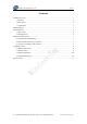
Wireless-Tag Technology Co., Ltd. V1.0.0 Contents 1 Module Overview.............................................................................................................................1 1.1 Features................................................................................................................................. 1 1.2 Description............................................................................................................................ 2 1.3 Applications..............
Wireless-Tag Technology Co., Ltd. V1.0.0 1 Module Overview 1.1 Features MCU ESP32-C3 chip embedded, 32-bit RISC-V single-core microprocessor, up to 160MHz ■ SRAM ■ RTC SRAM ■ ROM 400KB(16 KB for cache) 8KB 384KB WIFI IEEE 802.11b/g/n protocol Center frequency range of operating channel: 2400~2483.5 MHz Supports 20 MHz, 40 MHz bandwidth in 2.
Wireless-Tag Technology Co., Ltd. 40MHz crystal oscillator 4 MB SPI flash Operating voltage/Power supply: 3.0~3.6 V Operating ambient temperature: -40~85℃ Adopts DIP-11 package V1.0.0 1.2 Description WT32C3-01N is a general-purpose Wi-Fi and Bluetooth LE module. The rich set of peripherals and high performance make it an ideal choice for smart homes, industrial automation, health care, consumer electronics, etc.
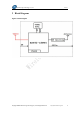
Wireless-Tag Technology Co., Ltd. V1.0.0 2 Block Diagram Figure 1 Block Diagram Copyright ©2020 Wireless-Tag Technology Co., Ltd. All Rights Reserved. http://www.wireless-tag.
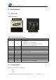
Wireless-Tag Technology Co., Ltd. V1.0.0 3 Pin Definitions 3.1 Pin Layout Figure 2 Pin Layout The pin descriptions are as follows. Table 1 Pin Definitions and Descriptions Pin Name Description Chip Enable pin: High level: on, enables the chip. Low level: off, the chip powers off, low current. Note: Do not leave the EN pin floating. 1 EN 2 IO1 GPIO1, ADC1_CH1, XTAL_32K_N (32.
Wireless-Tag Technology Co., Ltd. V1.0.0 GPIO9 Software can read the strapping values of these pins in “GPIO_STRAPPING” register. During the chip’s system reset(power-on-reset, RTC watchdog reset, brownout reset, analog super watchdog reset, crystal clock glitch detection reset), the latches of the strapping pins sample the voltage level as strapping bits of “0” or “1”, and hold these bits until the chip is powered down or shut down. By default, GPIO9 is connected to the internal pull-up resistor.
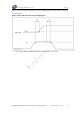
Wireless-Tag Technology Co., Ltd. V1.0.0 Figure 3 shows the setup and hold times for the strapping pin before and after the CHIP_EN signal goes high. Figure 3 Setup and Hold Times for the Strapping Pin Note: 1. The strapping combination of GPIO8 = 0 and GPIO9 = 0 is invalid. Copyright ©2020 Wireless-Tag Technology Co., Ltd. All Rights Reserved. http://www.wireless-tag.
Wireless-Tag Technology Co., Ltd. V1.0.0 4 Electrical Characteristics 4.1 Absolute Maximum Ratings Stresses above those listed in Absolute Maximum Ratings may cause permanent damage to the device. These are stress ratings only and functional operation of the device at these or any other conditions beyond those indicated under Recommended Operating Conditions is not implied. Exposure to absolute-maximum-rated conditions for extended periods may affect device reliability.
Wireless-Tag Technology Co., Ltd. V1.0.0 802.11n, HT20, MCS7, @17.5dBm 276 802.11n, HT40, MCS7, @17dBm 252 802.11b/g/n, HT20 84 802.11n, HT40 87 RX Note: 1. The current consumption measurements are taken with a 3.3 V supply at 25 °C of ambient temperature at the RF port. All transmitters’ measurements are based on a 100% duty cycle. 2. The current consumption figures in RX mode are for cases when the peripherals are disabled and the CPU is idle.
Wireless-Tag Technology Co., Ltd. V1.0.0 5 Application Note 5.1 Module Dimensions Figure 4 Module Dimensions 5.2 Reflow Profile Figure 5 Reflow Profile Copyright ©2020 Wireless-Tag Technology Co., Ltd. All Rights Reserved. http://www.wireless-tag.
Wireless-Tag Technology Co., Ltd. V1.0.0 5.3 Module Schematics Figure 6 Module Schematics Copyright ©2020 Wireless-Tag Technology Co., Ltd. All Rights Reserved. http://www.wireless-tag.
Wireless-Tag Technology Co., Ltd. V1.0.0 5.4 Peripheral Schematic This is the typical application circuit of the module connected with peripheral components (for example, power supply, antenna, reset button, JTAG interface, and UART interface). Figure 7 Application Circuit Note: Soldering the EPAD to the ground of the base board is not a must, though doing so can get optimized thermal performance. If you do want to solder it, please ensure that you apply the correct amount of soldering paste.
Wireless-Tag Technology Co., Ltd. V1.0.0 6 Product Trial Enquiry email:enquiry@wireless-tag.com Technical support email:technical@wireless-tag.com Copyright ©2020 Wireless-Tag Technology Co., Ltd. All Rights Reserved. http://www.wireless-tag.
Wireless-Tag Technology Co., Ltd. V1.0.0 Federal Communication Commission Statement (FCC, U.S.) This equipment has been tested and found to comply with the limits for a Class B digital device, pursuant to Part 15 of the FCC Rules. These limits are designed to provide reasonable protection against harmful interference in a residential installation.
Wireless-Tag Technology Co., Ltd. V1.0.0 equipment is no longer considered valid and the FCC ID of the module cannot be used on the final product. In these circumstances, the OEM integrator will be responsible for re-evaluating the end product (including the transmitter) and obtaining a separate FCC authorization. End product labeling: The final end product must be labeled in a visible area with the following: “Contains Transmitter Module FCC ID: 2AFOS-WT32C3-01N”.
Wireless-Tag Technology Co., Ltd. V1.0.0 integrates this module. The end user manual shall include all required regulatory information/warning as show in this manual. 2.4 Limited module procedures Not applicable. 2.5 Trace antenna designs Not applicable. The module has its own antenna, and doesn’t need a host’s printed board microstrip trace antenna etc. 2.
Wireless-Tag Technology Co., Ltd. V1.0.0 Operation Frequency: 2412~2462MHz Number of Channel: 11 Modulation: DSSS, OFDM Host manufacturer must perfom test of radiated & conducted emission and spurious emission, etc according to the actual test modes for a stand-alone modular transmitter in a host, as well as for multiple simultaneously transmitting modules or other transmitters in a host product.
Wireless-Tag Technology Co., Ltd. V1.0.0 Manufacturer's Name: Wireless-Tag Technology Co., Ltd Sample Description: WIFI Module Trade Mark: wireless-tag Model number: WT32C3-01N This device was tested for operations. To comply with RF exposure requirements, a minimum separation distance of 20cm must be maintained between the user’s body and the charger, including the antenna. Accessories that do not meet these requirements may not comply with RF exposure requirements and should be avoided.