Wireless-Tag Technology Co., Ltd. V1.0.0 WT32C3-S1 WT32C3-S2 Datasheet 2.4GHz WiFi (802.11b/g/n) and Bluetooth 5 module Built around ESP32-C3 series of SoCs,RISC-V single-core microprocessor 4MB flash On-board PCB antenna or external antenna connector V1.0.0 July 15, 2021 Wireless-Tag Technology Co., Ltd. I Copyright ©2020 Wireless-Tag Technology Co., Ltd. All Rights Reserved. http://www.wireless-tag.
Wireless-Tag Technology Co., Ltd. V1.0.0 About this document This document provides users with the technical specifications for WT32C3-S1 and WT32C3-S2. Document updates Please visit Wireless-Tag’s official website to download the latest version of the document. Revision history Please go to the document revision history page to view the revisions of the document. Disclaimer and copyright notice Information in this paper, including URL references, is subject to change without prior notice.
V1.0.0 Revision History No. Version Changes Change (+/-) Descriptions Author 1 V1.0.0 C Created the document Wang Date January 13, 2021 *Changes:C――create, A——add, M——modify, D——delete III Copyright ©2020 Wireless-Tag Technology Co., Ltd. All Rights Reserved. http://www.wireless-tag.
V1.0.0 Contents 1 Overview........................................................................................................................................................1 2 Features.......................................................................................................................................................... 2 3 Hardware Specifications................................................................................................................................ 3 3.
V1.0.0 1 Overview WT32C3-S1 and WT32C3-S2 are general-purpose Wi-Fi and Bluetooth low energy (Bluetooth LE) modules, which are embedded wireless network control modules with low power consumption and high cost performance. It can meet the needs of IoT applications such as smart grid, building automation, security, smart home, and telemedicine. WT32C3-S1 and WT32C3-S2 modules are equipped with 4 MB external SPI flash.
V1.0.0 2 Features QFN32 package On-board PCB antenna Operating voltage: 3.3V Operating ambient temperature: -20-85°C ESP32-C3 chip embedded, 32-bit RISC-V single-core microprocessor, up to 160MHz SRAM 400KB RTC SRAM 8KB ROM 384KB Embedded Flash System 4MB WIFI IEEE 802.11 b/g/n protocol 1T1R mode with data rate up to 150 Mbps WIFI @2.
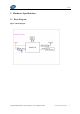
V1.0.0 3 Hardware Specifications 3.1 Block Diagram Figure 1 Block Diagram Copyright ©2020 Wireless-Tag Technology Co., Ltd. All Rights Reserved. http://www.wireless-tag.
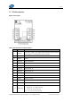
V1.0.0 3.2 Pin Descriptions Figure 2 Pin Layout Table 1 Pin Definitions and Descriptions Pin Name Description 1 VDD33 3.3V power supply; The output current delivered by the external power supply is recommended to be above 500mA. 2 GPIO6 GPIO6,FSPICLK,MTCK 3 GPIO9 GPIO9 4 GPIO10 GPIO10,FSPICS0 5 GPIO7 GPIO7,FSPID,MTDO 6 GND GND 7 GPIO18 GPIO18,USB_D- 8 GPIO19 GPIO18,USB_D+ 9 URXD GPIO20,U0RXD 10 GND GND 11 UTXD GPIO21,U0TXD 12 GPIO0 GPIO0.
V1.0.0 Pin Name Description 15 GPIO2 GPIO2,ADC1_CH2,FSPIQ 16 GPIO5 GPIO5,ADC2_CH0,FSPIWP,MTDI 17 GPIO4 GPIO4,ADC1_CH4,FSPIHD,MTMS 18 GND GND 3.3 Strapping Pins ESP32-C3 series has three strapping pins. GPIO2 GPIO8 GPIO9 Software can read the strapping values of these pins in “GPIO_STRAPPING” register.
V1.0.0 Pin Default Functionality When the value of eFuse field UART_PRINT_CONTROL is 0, print is enabled and not controlled by GPIO8. GPIO8 N/A 1, if GPIO8 is 0, print is enabled; if GPIO8 is 1, it is disabled. 2, if GPIO8 is 0, print is disabled; if GPIO8 is 1, it is enabled. 3, print is disabled and not controlled by GPIO8.
V1.0.0 4 Electrical Characteristics 4.1 Absolute Maximum Ratings Stresses above those listed in Absolute Maximum Ratings may cause permanent damage to the device. These are stress ratings only and functional operation of the device at these or any other conditions beyond those indicated under Recommended Operating Conditions is not implied. Exposure to absolute-maximum-rated conditions for extended periods may affect device reliability. 4.
V1.0.0 Table 5 Current Consumption Depending on Work Modes Work mode Modem-sleep Light-sleep Deep-sleep Power off Description The CPU is powered on 160MHz 80MHz EN is set to low level Copyright ©2020 Wireless-Tag Technology Co., Ltd. All Rights Reserved. Typical value 25.8mA 22.7mA 0.3mA 14uA 0 http://www.wireless-tag.
V1.0.0 5 Application Note 5.1 Module Dimensions Figure 4 Module Dimensions Copyright ©2020 Wireless-Tag Technology Co., Ltd. All Rights Reserved. http://www.wireless-tag.
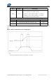
V1.0.0 5.2 Reflow Profile Figure 5 Reflow profile Copyright ©2020 Wireless-Tag Technology Co., Ltd. All Rights Reserved. http://www.wireless-tag.
V1.0.0 5.3 Module Schematics Figure 6 Module Schematics Copyright ©2020 Wireless-Tag Technology Co., Ltd. All Rights Reserved. http://www.wireless-tag.
V1.0.0 5.4 Peripheral Schematic This is the typical application circuit of the module connected with peripheral components (for example, power supply, antenna, reset button, JTAG interface, and UART interface). Figure 7 Application Circuit Soldering the EPAD to the ground of the base board is not a must, though doing so can get optimized thermal performance. If you do want to solder it, please ensure that you apply the correct amount of soldering paste.
V1.0.0 6 Product Trial Sales email:sales@wireless-tag.com Technical support email:technical@wireless-tag.com Copyright ©2020 Wireless-Tag Technology Co., Ltd. All Rights Reserved. http://www.wireless-tag.
Federal Communication Commission Statement (FCC, U.S.) This equipment has been tested and found to comply with the limits for a Class B digital device, pursuant to Part 15 of the FCC Rules. These limits are designed to provide reasonable protection against harmful interference in a residential installation. This equipment generates, uses and can radiate radio frequency energy and, if not installed and used in accordance with the instructions, may cause harmful interference to radio communications.
equipment is no longer considered valid and the FCC ID of the module cannot be used on the final product. In these circumstances, the OEM integrator will be responsible for re-evaluating the end product (including the transmitter) and obtaining a separate FCC authorization. End product labeling: The final end product must be labeled in a visible area with the following: “Contains Transmitter Module FCC ID: 2AFOS-WT32C3-SX”.
integrates this module. The end user manual shall include all required regulatory information/warning as show in this manual. 2.4 Limited module procedures Not applicable. 2.5 Trace antenna designs Not applicable. The module has its own antenna, and doesn’t need a host’s printed board microstrip trace antenna etc. 2.
WIFI Operation Frequency: 2412~2462MHz Number of Channel: 11 Modulation: DSSS, OFDM Host manufacturer must perfom test of radiated & conducted emission and spurious emission, etc according to the actual test modes for a stand-alone modular transmitter in a host, as well as for multiple simultaneously transmitting modules or other transmitters in a host product. Only when all the test results of test modes comply with FCC requirements, then the end product can be sold legally. 2.