Wireless-Tag Technology Co., Ltd. V1.0.0 WT32-S3-WROVER WT32-S3-WROVER-I Datasheet 2.4GHz WIFi(802.11b/g/n) and Buletooth 5(LE) module Built around ESP32-S3 series of SoCs,Xtensa dual-core 32-bit LX7 microprocessor Flash up to 16 MB,PSRAM up to 8MB On-board PCB antenna or external antenna connector V1.0.0 Sept 16, 2021 Wireless-Tag Technology Co., Ltd I Copyright ©2020 Wireless-Tag Technology Co., Ltd. All Rights Reserved. http://www.wireless-tag.
Wireless-Tag Technology Co., Ltd. V1.0.0 About this document This document provides users with the technical specifications for WT32-S3-WROVER1 and WT32-S3-WROVER2. Document updates Please visit Wireless-Tag’s official website to download the latest version of the document. Revision history Please go to the document revision history page to view the revisions of the document. Disclaimer and copyright notice Information in this paper, including URL references, is subject to change without prior notice.
Wireless-Tag Technology Co., Ltd. V1.0.0 Revision History No. Version Changes Change (+/-) Descriptions Author Date 1 V1.0.0 C First release Fiona Sept 16, 2021 *Changes:C――create, A——add, M——modify, D——delete III Copyright ©2020 Wireless-Tag Technology Co., Ltd. All Rights Reserved. http://www.wireless-tag.
Wireless-Tag Technology Co., Ltd. V1.0.0 Contents 1 Module Overview.............................................................................................................................1 1.1 Features................................................................................................................................. 1 1.2 Description............................................................................................................................ 2 1.3 Applications ............
Wireless-Tag Technology Co., Ltd. V1.0.0 1 Module Overview 1.1 Features MCU ESP32-S3 series of SoCs embedded,Xtensa® dual-core 32-bit LX7 microprocessor, up to 240MHz ■ SRAM ■ RTC SRAM ■ ROM ■ Up to 8 MB 512KB 16KB 384KB PSRAM WIFI IEEE 802.11b/g/n protocol Bit rate:802.11n uo to 150Mbps A-MPDU and A-MSDU aggregation 0.
Wireless-Tag Technology Co., Ltd. Operating voltage/Power supply: 3.0~3.6 V Operating ambient temperature: -40~85℃ Package size: (18 × 31 × 3.3) mm V1.0.0 1.2 Description WT32-S3-WROVER1 and WT32-S3-WROVER2 are two general-purpose Wi-Fi+Bluetooth low energy MCU modules, equipped with ESP32-S3 series chips.
Wireless-Tag Technology Co., Ltd. V1.0.0 1.
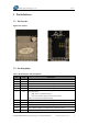
Wireless-Tag Technology Co., Ltd. V1.0.0 2 Block Diagram Figure 1 Block Diagram Copyright ©2020 Wireless-Tag Technology Co., Ltd. All Rights Reserved. http://www.wireless-tag.
Wireless-Tag Technology Co., Ltd. V1.0.0 3 Pin Definitions 3.1 Pin Layout Figure 2 Pin Layout 3.
Wireless-Tag Technology Co., Ltd. Pin Name V1.0.
Wireless-Tag Technology Co., Ltd. V1.0.0 3.3 Strapping Pins ESP32-S3 series has four strapping pins. GPIO0 = IO0 GPIO45 = IO45 GPIO46 = IO46 GPIO3=IO3 Software can read the strapping values of these pins in the register "GPIO_STRAPPING". During the system reset of the chip (power-on reset, RTC watchdog reset, brown-out reset, analog super watchdog reset, crystal oscillator clock glitch detection reset), the Strapping pin has the same function as the one on its own pin.
Wireless-Tag Technology Co., Ltd. V1.0.0 Pin Default SPI Boot Download Boot GPIO0 Pull-up 1 0 GPIO46 Pull-down Dot' 0 Pin IO46 Enabling/Disabling ROM Messages Print During Booting 3 4 Default Enabled Disabled Pull-down See the fourth note See the fourth note JTAG Signal Selection Pin Default EFUSE_DIS_USB_JTAG=0,EFUSE_DIS_PAD_JTAG=0, EFUSE_STRAP_JTAG_SEL=1 GPIO3 N/A 0:JTAG signal from on-chip JTAG pins 1:JTAG signal from USB Serial/JTAG controller Note: 1.
Wireless-Tag Technology Co., Ltd. V1.0.0 4 Electrical Characteristics 4.1 Absolute Maximum Ratings Table 4 Absolute maximum ratings Symbol Parameter Min Max Unit VDD33 Power supply voltage -0.3 3.6 V TSTORE Storage temperature -40 85 ℃ 4.2 Recommended Operating Conditions Table 5 Recommended Operating Conditions Symbol Parameter Min Typ Max Unit VDD33 Power supply voltage 3.0 3.3 3.6 V IV DD Current delivered by external power supply 0.
Wireless-Tag Technology Co., Ltd. V1.0.0 2. The current consumption figures in RX mode are for cases when the peripherals are disabled and the CPU is idle. Table 7 Current Consumption Depending on Work Modes Work mode Light-sleep Deep-sleep Hibernation Power off Description Typ Unit — 240 µA 8 µA 7 µA 1 µA RTC memory and RTC peripherals are powered on. RTC memory is powered on. RTC peripherals are powered off. CHIP_PU is set to low level. The chip is powered off.
Wireless-Tag Technology Co., Ltd. V1.0.0 5 Application Note 5.1 Module Dimensions Figure 3 Module Dimensions 5.2 Reflow Profile Figure 4 Reflow Profile Copyright ©2020 Wireless-Tag Technology Co., Ltd. All Rights Reserved. http://www.wireless-tag.
Wireless-Tag Technology Co., Ltd. V1.0.0 5.3 Peripheral Schematic This is the typical application circuit of the module connected with peripheral components (for example, power supply, antenna, reset button, JTAG interface, and UART interface). Figure 5 Module Schematics Copyright ©2020 Wireless-Tag Technology Co., Ltd. All Rights Reserved. http://www.wireless-tag.
Wireless-Tag Technology Co., Ltd. V1.0.0 5.4 Peripheral Design Schematic The application circuit diagram of the connection between the module and peripheral devices (such as battery, antenna, reset button, JTAG interface, UART interface, etc.). Figure 6 Application circuit diagram Copyright ©2020 Wireless-Tag Technology Co., Ltd. All Rights Reserved. http://www.wireless-tag.
Wireless-Tag Technology Co., Ltd. V1.0.0 6 Product Trial Enquiry email:enquiry@wireless-tag.com Technical support email:technical@wireless-tag.com Copyright ©2020 Wireless-Tag Technology Co., Ltd. All Rights Reserved. http://www.wireless-tag.
Federal Communication Commission Statement (FCC, U.S.) This equipment has been tested and found to comply with the limits for a Class B digital device, pursuant to Part 15 of the FCC Rules. These limits are designed to provide reasonable protection against harmful interference in a residential installation. This equipment generates, uses and can radiate radio frequency energy and, if not installed and used in accordance with the instructions, may cause harmful interference to radio communications.
equipment is no longer considered valid and the FCC ID of the module cannot be used on the final product. In these circumstances, the OEM integrator will be responsible for re-evaluating the end product (including the transmitter) and obtaining a separate FCC authorization. End product labeling: The final end product must be labeled in a visible area with the following: “Contains Transmitter Module FCC ID: 2AFOS-WT32S3WROVERX”.
integrates this module. The end user manual shall include all required regulatory information/warning as show in this manual. 2.4 Limited module procedures Not applicable. 2.5 Trace antenna designs Not applicable. The module has its own antenna, and doesn’ t need a host’ s printed board microstrip trace antenna etc. 2.
WIFI Operation Frequency: 2412~2462MHz Number of Channel: 11 Modulation: DSSS, OFDM Host manufacturer must perfom test of radiated & conducted emission and spurious emission, etc according to the actual test modes for a stand-alone modular transmitter in a host, as well as for multiple simultaneously transmitting modules or other transmitters in a host product. Only when all the test results of test modes comply with FCC requirements, then the end product can be sold legally. 2.