
User Manual
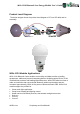


WiSe 1210 Bluetooth Low Energy Module User’s Guide
WiSilica Inc Proprietary and Confidential
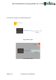
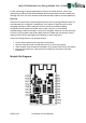
Module Pin Description
PINS NAME FUNCTION COMMENTS
TP1 SPI_MOSI I SPI data input or Programmable I/O
TP2 SPI_MISO O SPI data output or Programmable I/O
TP3 SPI_CSB O SPI select or Programmable I/O
TP4 SPI_PIO_SEL I Programmable I/O pulled high
TP5 3V3 Power Power Input
TP6 PIO[11] I/O Programmable I/O
TP7 PIO[10] I/O Programmable I/O
TP8 PIO[9] I/O Programmable I/O
TP9 SCL I/O Eeprom installed
TP10 SDA I/O Eeprom installed
TP11 PIO[3] I/O Programmable I/O
TP12 SPI_CLK I SPI Clock or Programmable I/O
TP13 PIO[4] O Programmable I/O
TP14 RX I/O Programmable I/O or UART RX
TP15 TX I/O Programmable I/O or UART TX
TP16 AIO[0] I/O Analog Programmable I/O
TP17 AIO[1] I/O Analog Programmable I/O
TP18 AIO[2] I/O Analog Programmable I/O
TP19 GND Ground Ground
Programmable GPIO’s
Totally 3 Analog Channels, 5 digital IO’s and 4 PWM channels are available in WiSe
1210 Module
ADC
WiSe 1210 Module supports 10bit ADC
• TP16 (AIO[0])
• T17 (AIO[1])
• TP18 (AIO[2])
Digital IO’s
• TP6 (PIO[11])
• TP7 (PIO[10])
• TP8 (PIO[9])
• TP11 (PIO[3])
• TP13 (PIO[4])