Product specification UMC-6270QV User Guide Wistron NeWeb Corp. CONFIDENTIAL THIS DOCUMENT CONTAINS PROPRIETARY TECHNICAL INFORMATION, WHICH IS THE PROPERTY OF THE WISTRON NEWEB CORPORATION AND SHALL NOT BE DISCLOSED TO OTHERS IN WHOLE OR IN PART, REPRODUCED, COPIED, OR USED AS THE BASIS FOR DESIGN, MANUFACTURING, OR SALE OF APPARATUS WITHOUT WRITTEN PERMISSION OF WISTRON NEWEB CORPORATION.
Product specification CONTENTS CONTENTS .......................................................................................................................................................................... 2 1. INTRODUCTION...................................................................................................................................................... 3 1.1 PRODUCT CONCEPT ..............................................................................................................
Product specification 1. INTRODUCTION This document describes the hardware interface of the WNC Small Form Factor (SFF) module used to connect the device application and the air interface. Two versions of Small Form Factor (SFF) module are described in this specification document as follows: 1.1 UMC-6270QV - HSDPA PRODUCT CONCEPT The SFF module is one of the smallest available WCDMA HSDPA of the market.
Product specification 1.3 TERMS AND ABBREVIATION ADC CODEC CLIP COLP CLIR COLR CTS CSD CS DCS DSR DTR ENS EONS ESD ETS FAX HSCSD HSDPA IC IEEE I/O ISO ITU JTAG Kbps LCD LED Mbps PBCCH PCB PCM PCS PWM RAM RF RI RMS RTS RX SIM SMS TBC TBD TX UART UMTS USB USIM USSD 1.
Product specification 1.5 PRODUCT FEATURES OVERVIEW Temperature range Normal range: -25°C to +85°C Storage: -40°C to +85°C Weight 6 g (typ.) ESD ESD protection >= 2 kV Physical dimensions 22.1 x 25.1 x 2.65 mm (typical) Connection 141 pin LGA type Power supply 3.4V to 4.2V range, 3.8V nominal Power consumption * Off mode: 50 µA typical Registered idle mode: WCDMA: 1.3 mA (DRX=9) Peak Current WCDMA: up to 700 mA Antenna /RF interface Both GPS and transmitter/receiver RF are LGA Pad.
Product specification • Data interface: USB2.0 Host High Speed • Form Factor: LGA module Specification • • • • • • • • • Communication Interface: (I2C x1/UART x1/USB2.0 x1/SPI x1/ SDIO x2) Support HSDPA (DL 3.6Mbps/UL 384Kbps) Supported SIM cards (3V and 1.8V SIM cards) USIM interface General purpose I/O pins ( x25) Audio Interface (PCM/ I2S) MCP (DDR 512Mb + 1Gb NAND) Support GPS RF interface: 2 RF pads for WCDMA TX/RX, and GPS.
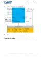
Product specification 2. BLOCK DIAGRAM & PIN ASSIGNMENT Pin Definition 4 This section is intended to capture the final LGA pin out for the SFF Module. The interfaces with a SFF module are all through a 141-pin surface LGA pad, as shown in Figure 2-1.
Product specification Figure 2-1: UMC-6270QV module Pin numbe Category r 1 RF 2 GND pin name WCDMA_A NT GND Pad Pad type Description group AI,AO WCDMA antenna signal GND 8 Driving capacity
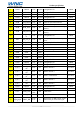
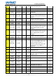
Product specification 3 GPIO GPIO9 1.8V I/O, PD Configurable I/O 1-8mA 4 GPIO GPIO2 1.8V I/O, PD Configurable I/O 1-8mA 5 GPIO GPIO5 1.8V I/O, PD Configurable I/O 1-8mA 6 GPIO GPIO8 1.8V I/O, PD Configurable I/O 1-8mA 7 I2C I2C_SCL 1.8V I/O I2C clock 8 PCM PCM_BCLK 1.8V DO Clock for the PCM interface 9 PCM PCM_SYNC 1.8V DO 10 PCM PCM_DIN 1.8V DI 11 PCM PCM_DOUT 1.
Product specification 34 JTAG 35 JTAG 36 JTAG 37 38 39 40 41 JTAG_TMS 1.8V JTAG_RTCK 1.8V DI, PU JTAG test mode select DO 1.8V DI, PU JTAG clock input 1.8V/2 UICC USIM_DAT I/O USIM data .85V External supply voltage; connect power input USB_VBUS P directly to the external USB power supplier power 1.8V/2 USIM_VREG P Output of the linear regulators output .
Product specification 58 GPIO GPIO11 1.8V I/O, PD Configurable I/O 1-8mA 59 GPIO GPIO24 1.8V I/O, PD Configurable I/O 1-8mA 60 GND GND 61 GPIO GPIO18 1.8V I/O, PD Configurable I/O 1-8mA 62 GPIO GPIO15 1.8V I/O, PD Configurable I/O 1-8mA 63 GPIO GPIO7 1.8V I/O, PD Configurable I/O 1-8mA 64 GPIO GPIO1 1.8V I/O, PD Configurable I/O 1-8mA 65 I2C I2C_SDA 1.8V I/O 66 UART UART_TX 1.8V DO 67 UART UART_RFR 1.8V DO 68 UART UART_RX 1.
Product specification 88 SDIO1 89 SDIO1 90 GPIO 91 GND 92 93 UICC 94 JTAG 95 JTAG power output 96 97 98 99 100 101 102 103 104 105 106 107 GND 109 Speaker 110 Speaker 112 113 GPIO3 1.8V I/O SDIO1 data bit 1 2-16mA DO Output clock for SDIO1 device 2-16mA I/O, PU Configurable I/O GND GND WLAN_PWR 2.6V I/O, PU Configurable I/O _DOWN 1.8V/2 USIM_RST DO USIM reset .85V JTAG_TDO 1.8V Z JTAG test data output JTAG_TDI 1.8V DI, PU JTAG test data input VREG_MSM 2.
Product specification DI, DO 114 115 116 current sink VIB_DRV_N ADC in HKAIN1 current sink LCD_DRV_N AI Connect to the vibration motor (-) terminal. The (+) terminal of the motor connects to VDD AI ADC input AI Connect to the LCD backlight (-) terminal. The (+) terminal of the LCD backlight connects to VDD 150mA 117 GND GND GND 118 GPIO GPIO13 1.8V I/O, PD Configurable I/O 1-8mA 119 GPIO GPIO0 1.8V I/O, PD Configurable I/O 1-8mA 120 GPIO GPIO12 1.
Product specification 3. RF AIR INTERFACES AND PERFORMANCE 3.1 RF AIR INTERFACE AND BAND CONFIGURATION 3.1.1 Air interfaces UMC-6270QV module supports WCDMA R99, HSDPA and GPS 3.2 RF PERFORMANCE The UMC-6270QV modules RF transmitter/receiver is fully compliant with the applicable standards. The sensitivity and max output power are listed in Table 3-2-1 and Table 3-2-2 Specification Min Typ Max Units -104.7 -108 dBm -106.
Product specification 4. OPERATING CONDITIONS 4.1 ABSOLUTE MAXIMUM RATINGS Operating UMC-6270QV Modules under conditions beyond its absolute maximum ratings (Table 4-1) may damage the device. Absolute maximum ratings are limiting values to be considered individually when all other parameters are within their specified operating ranges. Functional operation and specification compliance under any absolute maximum condition, or after exposure to any of these conditions, is not guaranteed or implied.
Product specification 4.2 RECOMMENDED OPERATING CONDITION The devices meet all performance specifications when used within the recommended operating conditions as described in Table 4-2 Symbol T Parameter Min Typ. Max -25 +85 -20 +65 -25 -20 +65 +85 Unit USB_VBUS Operating Temperature Normal operating temperature range See section 4.2.1 Extended operating temperature range 1 See section 4.2.2 Extended operating temperature range 2 See section 4.2.3 DC Power Supply Voltage 4.75 5 5.
Product specification 5. CURRENT CONSUMPTION The specified supply currents in Table 5-1 are based operation at room temperature. Current measurements are taken with default parameter settings, nominal supply voltage. The DUT is mounted on a module test board and the accelerometer on, unless otherwise noted.
Product specification 6. APPLICATION DESIGN NOTES 6.1 Layout Notes 6.1.1 RF Pin Input Impedance Matching Applications utilizing the module must ensure that a 50Ω controlled impedance trace is used. Shown in the accompanying table are example calculations for a four- layer FR4 stack up and the resulting trace width for Bluetooth RF input. The figure below illustrates the layer stack up for a four- layer board according to the Description column in the table below.
Product specification 6.1.
Product specification 7. MECHANICAL REQUIREMENTS 7.
Product specification Figure 7-1-2 Recommended Footprint of SFF Module 21
Product specification 8 Certification Requirements 8.1 Carrier Certification Requirements The SFF Development Kit will be used to demonstrate Safe for Network (SFN) compliance for the SFF module on selected cellular carriers. 8.2 Regulatory Compliance 5 8.3 FCC warning statement FCC Regulations: This device complies with Part 15 of the FCC Rules.
Product specification Radiation Exposure Statement: This equipment complies with FCC radiation exposure limits set forth for an uncontrolled environment. This equipment should be installed and operated with minimum distance 20cm between the radiator & your body. This device is intended only for OEM integrators under the following conditions: 1) The antenna must be installed such that 20 cm is maintained between the antenna and users, and the antenna gain allowed for use with this device is 2 dBi.