
User's Manual


Product specification
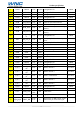
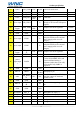
10
34
JTAG
JTAG_TMS
1.8V
DI, PU
JTAG test mode select
35
JTAG
JTAG_RTCK
1.8V
DO
JTAG return clock
36
JTAG
JTAG_TCK
1.8V
DI, PU
JTAG clock input
37
UICC
USIM_DAT
1.8V/2
.85V
I/O
USIM data
38
power input
USB_VBUS
P
External supply voltage; connect
directly to the external USB power
supplier
39
power
output
USIM_VREG
1.8V/2
.85V
P
Output of the linear regulators
150mA
40
GND
GND
GND
41
GND
GND
GND
42
power input
VCHG
P
External supply voltage; connect
both pins directly to the external
power supply (such as a wall
charger).
43
power input
VCHG
P
External supply voltage; connect
both pins directly to the external
power supply (such as a wall
charger).
44
power
output
VREG_MSM
E
1.8V
300mA
Output of the linear regulators
45
GND
GND
GND
46
power
input/outpu
t
VCOIN
P
Used as an analog input from the 3
V coin cell for SMPL, RTC,and
crystal oscillator backup; a
capacitor (rather than a coin cell)
can be used if only SMPL is
supported
47
GND
GND
GND
48
ADC in
MPP3
AI,AO,
DI, DO
multipurpose pin
49
other
PON_REST_
N
1.8V
DO
Connected internally to RESIN_N;
logic low causes the baseband
circuits to reset.
50
GND
GND
GND
51
ADC in
BATT_THER
M
AI
connect to battery package thermal
pin
52
GND
GND
GND
53
microphone
MIC_P
AI
Microphone #1 input (+)
54
microphone
MIC_M
AI
Microphone #1 input (-)
55
GND
GND
GND
56
GPIO
GPIO4
1.8V
I/O, PD
Configurable I/O
1-8mA
57
GPIO
GPIO6
1.8V
I/O, PU
Configurable I/O
1-8mA