7
2. BLOCK DIAGRAM & PIN ASSIGNMENT
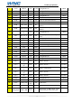
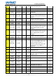
Pin Definition 4
This section is intended to capture the final LGA pin out for the SFF Module.
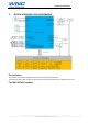
The interfaces with a SFF module are all through a 141-pin surface LGA pad, as shown in Figure 2-1.
For UMC-6270QV module: