
Product Specs


4
□文件新增 Addition of Document ■文件變更 Alteration of Document □文件作廢 Revocation of Document
Subject: Doc. No.: Rev: 2
UMC-STD31LF Product Specification Page 3 of 54
本資料為啟碁科技股份有限公司專有之財產,非經書面許可,不准透露或使用本資料,亦不准複印,複製或轉變成其他形式使用。
The information contained herein is the exclusive property of WNC and shall not be distributed, reproduced, or disclosed in whole or in part without prior written permission from WNC.
Form No.: 2-JT-00022-03_001
UMC-STD31LF Product Specification
3
1.1 Regional variant ....................................................................................................................................... 5
1.2 Performance key features ........................................................................................................................ 5
1.3 Interface ................................................................................................................................................... 6
1.3.1 Signal interface ................................................................................................................................. 6
1.3.2 GPIO .................................................................................................................................................. 6
1.3.3 Antenna interface ............................................................................................................................. 6
1.3.4 Power input interface ....................................................................................................................... 6
1.3.5 Power output interface ..................................................................................................................... 7
1.4 Operation condition ................................................................................................................................. 7
1.5 Mechanical specification.......................................................................................................................... 7
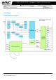
2 Block diagram .................................................................................................................................................. 8
2.1 UMC-STD31LF block diagram ................................................................................................................... 8
2.2 Software stack .......................................................................................................................................... 9
3 Board placement ............................................................................................................................................. 9
3.1 Top side .................................................................................................................................................... 9
3.2 Bottom side ............................................................................................................................................ 10
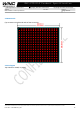
3.3 Pin diagram ............................................................................................................................................ 10
3.5 GPIO table .............................................................................................................................................. 24
3.5.1 Alternate Function .............................................................................................................................. 24
3.5.2 Wake up/De-bounce ........................................................................................................................... 27
4 Mechanical design ........................................................................................................................................ 30
4.1 Shielding case design ............................................................................................................................. 30
4.2 Label information ................................................................................................................................... 31
4.3 NAD land pattern ................................................................................................................................... 32
4.4 Stencil opening ....................................................................................................................................... 32
4.5 Reflow profile ......................................................................................................................................... 33
4.6 Moisture sensitivity level ....................................................................................................................... 33
4.7 ESD ......................................................................................................................................................... 34
4.8 Packaging ............................................................................................................................................... 34
5 Thermal design .............................................................................................................................................. 36
5.1 Thermal sensor ...................................................................................................................................... 36
5.2 Software thermal mitigation .................................................................................................................. 37
6 RF specification ............................................................................................................................................. 38
6.1 UMC-STD31LF ........................................................................................................................................ 38
6.1.1 Maximum output power ................................................................................................................. 38
6.1.2 Sensitivity limit ................................................................................................................................ 38
7 Evaluation Kit ................................................................................................................................................ 39
8 Design application notes ............................................................................................................................... 41
8.1 Power trace ............................................................................................................................................ 41
8.2 Power ON/OFF and Reset ...................................................................................................................... 41
8.2.1 Power ON ........................................................................................................................................ 41
8.2.2 Power OFF ....................................................................................................................................... 41