
Data Sheet

Data Sheet
©2013
Würth Elektronik eiSos GmbH & Co. KG - REV 0.2
PRELIMINARY
14/ 25
171012401/WPMDH1102401J
MagI³C Power Module Product Family
VDRM - Variable Step Down Regulator Module
J CIRCUIT DESCRIPTION
The feed forward capacitor C
FF
, should be located close to the FB pin.
Power loss and board thermal requirements
For example:
, the device must see a maximum junction-to-ambient thermal resistance of:
(17)
This
will ensure that the junction temperature of the regulator does not exceed
in the particular
application ambient temperature.
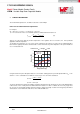
To calculate the required
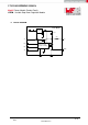
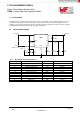
we need to get an estimate for the power losses in the IC. The following graph is
taken form the typical performance characteristics section and shows the power dissipation of the power module for
V
OUT
= 12V at 85°C T
AMB
.
Power Loss [W]
Output Current [A]
Power Loss: V
OUT
= 12V @ T
AMB
= 85°C
0.0
0.3
0.6
0.9
1.2
1.5
0.0 0.2 0.4 0.6 0.8 1.0
V
IN
= 15V
V
IN
= 24V
V
IN
= 36V
Using the 85°C T
AMB
power dissipation data as a conservative starting point, the power dissipation PD for
and
is estimated to be 0.75W. The necessary
can now be calculated.
To achieve this thermal resistance the PCB is required to dissipate the heat effectively. The area of the PCB will have
a direct effect on the overall junction-to-ambient thermal resistance. In order to estimate the necessary copper area
we can refer to the following package thermal resistance graph. This graph is taken from the typical performance
characteristics section and shows how the
varies with the PCB area.