
Data Sheet

Data Sheet
©2013
Würth Elektronik eiSos GmbH & Co. KG - REV 0.2
PRELIMINARY
15/ 25
171050601/WPMDM1500602J
MagI³C Power Module Product Family
VDRM - Variable Step Down Regulator Module
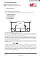
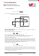
J CIRCUIT DESCRIPTION
For example:
the device must see a maximum junction-to-ambient thermal resistance of:
(10)
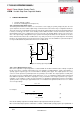
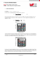
Given the typical thermal resistance from junction to case to be 1.9°C/W. Use the 85°C power dissipation curves in
the typical performance characteristics section to estimate the P
IC-LOSS
for the application being designed. In this
application it is 5.5W.
0 1 2 3 4 5
V
IN
= 9V
V
IN
= 12V
V
IN
= 24V
V
IN
= 36V
Power Loss [W]
Output Current [A]
Power Loss: V
OUT
= 3.3V @ T
AMB
= 85°C
0
1
2
3
4
5
6
7
8
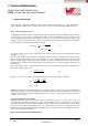
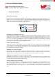
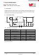
To achieve this thermal resistance the PCB is required to dissipate the heat effectively. The area of the PCB will have
a direct effect on the overall junction-to-ambient thermal resistance. In order to estimate the necessary copper area
we can refer to the following package thermal resistance graph. This graph is taken from the typical performance
characteristics section and shows how the
varies with the PCB area.
Thermal Resistance θ
JA
[°C/W]
Board Area [cm²]
Package Thermal Resistance θ
JA
4 Layer
Printed Circuit Board with 35µm Copper
0LFM (0m/s) air
225LFM (1.14m/s) air
500LFM (2.54m/s) air
Evaluation Board Area
0
5
10
15
20
25
30
35
40
0 10 20 30 40 50 60
For
and only natural convection (i.e. no air flow), the PCB area can be smaller than 18cm
2
. This
corresponds to a square board with 3cm x 3cm copper area, 4 layers, and 35µm copper thickness. Higher copper
thickness will further improve the overall thermal performance. Note that thermal vias should be placed under the IC
package to easily transfer heat from the top layer of the PCB to the inner layers and the bottom layer.