
Data Sheet

Data Sheet
©2013
Würth Elektronik eiSos GmbH & Co. KG - REV 0.2
PRELIMINARY
16/ 25
171050601/WPMDM1500602J
MagI³C Power Module Product Family
VDRM - Variable Step Down Regulator Module
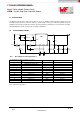
J CIRCUIT DESCRIPTION
PCB Layout Instructions:
PC board layout is an important part of DC-DC converter design. Poor board layout can disrupt the performance of a
DC-DC converter and surrounding circuitry by contributing to EMI, ground bounce and resistive voltage drop in the
traces. These can send erroneous signals to the DC-DC converter resulting in poor regulation or instability. Good
layout can be implemented by following five simple design rules.
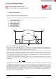
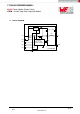
C
IN
V
IN
VIN
AGND
VOUT
Power Module
C
OUT
V
OUT
Loop 1
Loop 2
High
di/dt
1: Minimize area of switched current loops.
From an EMI reduction standpoint, it is imperative to minimize the high di/dt paths during PC board layout. The high
current loops that do not overlap have high di/dt content that will cause observable high frequency noise on the
output pin if the input capacitor (C
in1
) is placed at a distance away from the MagI³C power module. Therefore place
C
IN1
as close as possible to the MagI³C power module V
IN
and PGND exposed pad. This will minimize the high di/dt
area and reduce radiated EMI. Additionally, grounding for both the input and output capacitor should consist of a
localized top side plane that connects to the PGND exposed pad.
2: Have a single point ground.
The ground connections for the feedback, soft-start, and enable components should be routed to the GND pin of the
device. This prevents any switched or load currents from flowing in the analog ground traces. If not properly handled,
poor grounding can result in degraded load regulation or erratic output voltage ripple behavior. Provide the single
point ground connection from pin 4 to PGND.
3: Minimize trace length to the FB pin.
The feedback resistors, R
FBT
and R
FBB
, and the feed forward capacitor C
FF
, should be located close to the FB pin.
Since the FB node is high impedance, maintain the copper area as small as possible. The traces from R
FBT
, R
FBB
,
and C
FF
should be routed away from the body of the MagI³C power module to minimize noise pickup.
4: Make input and output bus connections as wide as possible.
This reduces any voltage drops on the input or output of the converter and maximizes efficiency. To optimize voltage
accuracy at the load, ensure that a separate feedback voltage sense trace is made to the load. Doing so will correct
for voltage drops and provide optimum output accuracy.
5: Provide adequate device heat-sinking.
Use an array of heat-sinking vias to connect the exposed pad to the ground plane on the bottom PCB layer. If the
PCB has a plurality of copper layers, these thermal vias can also be employed to make connection to inner layer
heat-spreading ground planes. For best results use a 6 x 10 via array with minimum via diameter of 254μm thermal
vias spaced 1mm. Ensure enough copper area is used for heat-sinking to keep the junction temperature below
125°C.