Virtex-II Prototype Platform User Guide UG015 / PN0401974 (v1.
Virtex-II Prototype Platform www.xilinx.com 1-800-255-7778 UG015 / PN0401974 (v1.
R "Xilinx" and the Xilinx logo shown above are registered trademarks of Xilinx, Inc. Any rights not expressly granted herein are reserved. CoolRunner, RocketChips, Rocket IP, Spartan, StateBENCH, StateCAD, Virtex, XACT, XC2064, XC3090, XC4005, and XC5210 are registered trademarks of Xilinx, Inc. The shadow X shown above is a trademark of Xilinx, Inc. ACE Controller, ACE Flash, A.K.A.
Virtex-II Prototype Platform UG015 / PN0401974 (v1.1) January 14, 2003 The following table shows the revision history for this document. Version Revision 06/29/01 1.0 Initial Xilinx release. 01/14/03 1.1 Trademark updates and correction to VCCO Supply Jumpers section. Virtex-II Prototype Platform www.xilinx.com 1-800-255-7778 UG015 / PN0401974 (v1.
Table of Contents Preface: About This Manual Additional Resources . . . . . . . . . . . . . . . . . . . . . . . . . . . . . . . . . . . . . . . . . . . . . . . . . . . . . . . . 7 Conventions . . . . . . . . . . . . . . . . . . . . . . . . . . . . . . . . . . . . . . . . . . . . . . . . . . . . . . . . . . . . . . . . . 8 Typographical . . . . . . . . . . . . . . . . . . . . . . . . . . . . . . . . . . . . . . . . . . . . . . . . . . . . . . . . . . . . . 8 Online Document . . . . . . . . . . . . . . . . .
R 20. Pin Breakout . . . . . . . . . . . . . . . . . . . . . . . . . . . . . . . . . . . . . . . . . . . . . . . . . . . . . . . . . . 21. User LEDs (Active-High) . . . . . . . . . . . . . . . . . . . . . . . . . . . . . . . . . . . . . . . . . . . . . . . 22. Program Switch . . . . . . . . . . . . . . . . . . . . . . . . . . . . . . . . . . . . . . . . . . . . . . . . . . . . . . . 23. Reset Switch (Active-Low) . . . . . . . . . . . . . . . . . . . . . . . . . . . . . . . . . . . . . . . . . . . . . . 24.
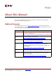
R Preface About This Manual This document describes the features and operation of Virtex-II Prototype Platform prototype and demonstration boards. Additional Resources For additional information, go to http://support.xilinx.com. The following table lists some of the resources you can access from this website. You can also directly access these resources using the provided URLs.
R Preface: About This Manual Conventions This document uses the following conventions. An example illustrates each convention.
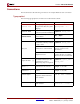
R Conventions Online Document The following conventions are used in this document: Convention Meaning or Use Example Blue text Cross-reference link to a location in the current file or in another file in the current document See the section “Additional Resources” for details. Red text Cross-reference link to a location in another document See Figure 2-5 in the Virtex-II Handbook. Blue, underlined text Hyperlink to a website (URL) Go to http://www.xilinx.com for the latest speed files.
R 10 Preface: About This Manual www.xilinx.com 1-800-255-7778 Virtex-II Prototype Platform UG015 / PN0401974 (v1.
R Virtex-II Prototype Platform Package Contents • Xilinx Virtex™-II Prototype Platform board • User guide • Device vacuum tool • BNC to SMB cable • Headers for test points • CD-ROM CD-ROM Contents • User guide in PDF format • Example design demonstration that flashes the on-board LED. This design includes the Verilog source code, demo.v, demo.ucf, and a readme.txt file • Bitstream files (*.
R • Four global clock (GCLK) inputs ♦ two 50Ω SMB connectors ♦ two LVTTL-type oscillator sockets • On-board programmable oscillator • Selectable on-board clock frequency (from 25 MHz to 90 MHz) • Power indicator LED • 44-pin, VQFP PROM socket for any configuration mode • JTAG port for reprogramming the XC17Vxx and XC18Vxx series reconfigurable PROMs and the User FPGA (DUT) • Upstream and downstream System ACE and Configuration Interface connectors • On-board battery holder The kit contai
R Introduction Figure 1 shows a block diagram of the board.
R Detailed Description The Virtex-II Prototype Platform board is shown in Figure 2. Each feature is detailed in the numbered sections that follow. 5a 5c 17 3 10 1 18 9 1a 2 11 8 20 16 15 19 4 12 5 6 22 23 7 13 14 24 21 25 5b 5d Figure 2: Detailed Description of Virtex-II Prototype Platform Components 1. Power Switch The board has an on-board power supply and a three-position power switch: upward on, off, and downward on.
R Detailed Description Table 1: Voltage Ranges Label Max Voltage Min Voltage VCCINT 1.5V 1.3V VCCO 3.3V 2.5V VCCAUX 3.3V 2.5V Off Position In the off position, the power switch disables all modes of powering the DUT in standalone operation. Downward On Position In the downward on position, the power switch enables delivery of all power from the six power supply jacks. 2.
R 3. Configuration Port User PROM and FPGA Header This header is used to connect a MultiLINX cable or Parallel Cable III cable to the board and supports all Virtex-II device configuration modes. (See Table 4 for connecting cables to the Configuration Port User PROM and FPGA header.) 4. Frequency Select Switch The frequency select switch sets the frequency of the on-board clock generator. One of sixteen frequencies can be selected as shown in Table 2.
R Detailed Description In either of the master serial configuration modes, the CCLK and DIN (D0) signals are routed to the Downstream Configuration Interface connector to allow daisy-chaining to downstream slave serial devices. Note: Only one master serial device is allowed in a chain and it must be the first FPGA device in the stream. In master select map modes, the CCLK and D0-D7 signals are routed to the Downstream Configuration Interface connector to allow daisy-chaining to downstream devices.
R devices. When configuring from the Upstream Configuration Interface connector, the M0M2, CS, and RW signals are set by the Upstream Configuration Interface connector or the Configuration User PROM and FPGA header pins. Table 5 shows the Configuration Port User PROM and FPGA header pins on the board and the corresponding pins for connecting the MultiLINX cable for select map mode.
R Detailed Description the on-board PROM and the DUT. TDI is a serial JTAG chain input and TDO is a serial JTAG chain output. Note: The DOWNSTREAM_TDO TERM switch must be set to the “on” position on the last board in the chain to connect the TDO pin of the final device to the TDO feedback chain.
R must be provided by the user. The only services provided by the board in this mode are the on-board oscillators, the DONE and INIT LEDs, and VBATT. All connections to the configuration pins must be made using the breakout test points. 5a. Upstream System ACE Connector The Upstream System ACE connector, as shown in Figure 3, can be used to configure the DUT. This connector can be sourced by any JTAG configuration stream.
R Detailed Description 5c. Upstream Configuration Interface Connector The Upstream Configuration Interface connector, as shown in Figure 5, is used to configure the DUT in select-map or slave-serial mode. This connector can only be sourced by a the Downstream Configuration Interface connector of another prototype platform.
R 5d. Downstream Configuration Interface Connector The Downstream Configuration Interface connector, as shown in Figure 6, passes selectmap or slave-serial configuration information to a DUT in a downstream prototype platform from sources such as a MultiLINX cable or a Parallel Cable III.
R Detailed Description 7. Chip Select Switch The chip select switch assigns a unique identification (ID) to each DUT in a select map configuration chain. This switch may be set from 0 to 3, allowing up to four devices to be configured/read back in a select map chain. During readback, each board in the chain must have a unique ID, otherwise more than one device will drive the data bus. However, multiple DUTs may be set to the same ID for “Select Map Mode” configuration.
R 12. Prototyping Area The prototyping area accommodates 0.10" spaced ICs. The kit contains headers that can be soldered to the breakout area, if desired. Power and ground buses are located at the top and bottom, respectively, of the prototyping area. 13. VCCO Supply Jumpers Virtex-II series devices have eight SelectIO banks, labeled 0 through 7, each with a VCCO supply. VCCO_EN supply jumpers can connect each bank to one of the three on-board supplies, VCCINT, VCCO, or externally from VIO.
R Detailed Description 17. Clock Enable Switches 0-7 The user has access to eight additional global clocks on the DUT. These clocks can be enabled by setting the appropriate dip switches shown in Table 10. After selecting the clock frequency, all enabled clocks run at that frequency.
R 19. DUT Socket The DUT socket contains the user FPGA, referred to as the Device Under Test. The device must be oriented using the P1 indicator on the board. Failure to insert the device to the proper orientation can damage the device. To avoid pin damage, always use the vacuum tool provided when inserting or removing the Virtex-II device. When using BGA packages, do not apply pressure to the device while activating the vacuum tool lever. Doing so can damage the socket and/or the device. 20.
R Detailed Description Table 13: LED Assignments and Corresponding I/O (Continued) Configuration Mode Status LED Before and During Configuration After Configuration Pin Number For Package Type Status Pin FG256 FG456 FG676 FF1152 LED 6 Select Map D6 R4 AB4 AD6 AG24 LED 7 DLL Locked Status D7 P4 AA4 AC6 AG25 22. Program Switch The active-low program switch, when pressed, grounds the program pin on the DUT. This switch is driven indirectly by the Service FPGA. 23.
R User Programmable Pins Table 14 shows the user hardware that corresponds to available DUT package types.
R User Programmable Pins Table 15: Clock Pins and Corresponding I/Os (Continued) FG256 Clock Pins Clock Name Pin Number FG456 Clock Name Pin Number FG676 Clock Name Pin Number FF1152 Clock Name Pin Number Breakout Area 3 GCLK7S T8 GCLK7S AA11 GCLK7S AC13 GCLK7S AK18 Breakout Area 4 GCLK0P T9 GCLK0P AB12 GCLK0P AD14 GCLK0P AK17 Virtex-II Prototype Platform UG015 / PN0401974 (v1.1) January 14, 2003 www.xilinx.