
User manual

Virtex-II Prototype Platform www.xilinx.com 17
UG015 / PN0401974 (v1.1) January 14, 2003 1-800-255-7778
Detailed Description
R
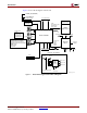
In either of the master serial configuration modes, the CCLK and DIN (D0) signals are
routed to the Downstream Configuration Interface connector to allow daisy-chaining to
downstream slave serial devices.
Note:
Only one master serial device is allowed in a chain and it must be the first FPGA device in the
stream.
In master select map modes, the CCLK and D0-D7 signals are routed to the Downstream
Configuration Interface connector to allow daisy-chaining to downstream devices.
Note:
For more details on configuration modes, consult the Xilinx Data Book located at:
http://www.xilinx.com/partinfo/databook.htm
.
Master Serial PROM Mode
In switch position 0 (Master Serial PROM) the on-board PROM is used as the configuration
data source.
Master Serial UPSTREAM Mode
In switch position 1 (Master Serial UPSTREAM) the Upstream Configuration Interface
connector or the Configuration User PROM and FPGA header can be used as the
configuration data source. All configuration signals from/to the DUT are then routed
accordingly.
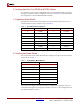
Table 4 shows the Configuration Port User PROM and FPGA header pins on the board and
the corresponding pins for connecting MultiLINX or Parallel Cable III cables for serial
mode.
Master Select Map PROM Mode
In switch position 2 (Master Select Map PROM) the on-board PROM or PROM daughter
card interface is used as the configuration data source for the DUT. The PROM, the M0-
M2, CS, and the RW signals are set by the Service FPGA.
Master Select Map UPSTREAM Mode
In switch position 3 (Master Select Map UPSTREAM) the Upstream Configuration
Interface connector or the Configuration Port User PROM and FPGA header can be used as
a configuration data source for the DUT. All configuration signals from/to the DUT are
then routed accordingly. In this mode, the CCLK and D0-D7 are routed to the
Downstream Configuration Interface connector to allow daisy-chaining to downstream
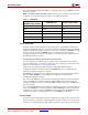
Table 4: Serial Mode
Configuration Port User
PROM and FPGA Header
MultiLINX Pins Parallel Cable III Pins
VCC3 PWR VCC
GND GND GND
CCLK CCLK CCLK
DONE DONE D/P
D0 DIN DIN
PROG PROG PROG
INIT INIT