
User manual

18 www.xilinx.com Virtex-II Prototype Platform
1-800-255-7778 UG015 / PN0401974 (v1.1) January 14, 2003
R
devices. When configuring from the Upstream Configuration Interface connector, the M0-
M2, CS, and RW signals are set by the Upstream Configuration Interface connector or the
Configuration User PROM and FPGA header pins.
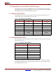
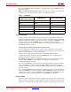
Table 5 shows the Configuration Port User PROM and FPGA header pins on the board and
the corresponding pins for connecting the MultiLINX cable for select map mode.
Slave Serial Mode
In switch position 4 (Slave Serial) either the Upstream Configuration Interface connector or
the Configuration Port User PROM and FPGA header are used as a configuration data
source for configuring the DUT in slave serial format. In this mode, the upstream device
supplies the CCLK and DIN signals, as well as all other configuration signals to the DUT.
(See Table 4 for connecting to the Configuration Port User PROM and FPGA header.)
JTAG Mode
In switch position 5 (JTAG) the System ACE connectors to upstream and downstream
boards are selected. Each System ACE connector contains pins for each of the four JTAG
signals: TCK, TMS, TDI, and TDO.
TCK and TMS are parallel feedthrough connections from the upstream System ACE
connector to the downstream System ACE connector and drive the TCK and TMS pins of
Table 5: Select Map Mode
Configuration Port User
PROM and FPGA Header
MultiLINX Pins
VCC3 PWR
GND GND
CCLK CCLK
DONE DONE
PROG PROG
INIT INIT
CS0 CS0 (CS)
RDWR RS (RDWR)
DOUT RDY/BUSY
D0 D0
D1 D1
D2 D2
D3 D3
D4 D4
D5 D5
D6 D6
D7 D7