
User manual

Virtex-II Prototype Platform www.xilinx.com 19
UG015 / PN0401974 (v1.1) January 14, 2003 1-800-255-7778
Detailed Description
R
the on-board PROM and the DUT. TDI is a serial JTAG chain input and TDO is a serial
JTAG chain output.
Note:
The DOWNSTREAM_TDO TERM switch must be set to the “on” position on the last board in
the chain to connect the TDO pin of the final device to the TDO feedback chain.
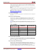
Select Map Mode
In switch position 6 (Select Map) the configuration data is supplied byte wide from the
Upstream Configuration Interface connector or from the Configuration Port User PROM
and FPGA Header and requires an external clock source. The mode pins M0-M2 are set by
the Service FPGA. The CS and RDWR signals are generated from the Upstream
Configuration Interface connector. (See Table 5 for connecting to the Configuration Port
User PROM and FPGA header.)
Configuration/Readback from the Upstream Connector
To use configuration/readback mode, you must set the configuration mode switch to
position 6 (Select Map). You must also set the chip select switch to provide each device in
the chain a unique ID. (See “7. Chip Select Switch”.)
In this mode of configuration, byte-wide data is obtained from the Upstream
Configuration Interface connector. The CS and RDWR pins are also supplied by the
Upstream Configuration Interface connector.
The RDWR pin on the Upstream Configuration Interface connector determines the data
direction. When RDWR is low, the data flows from the DUT to the Upstream
Configuration Interface connector.
The value of the INIT pin on the Upstream Configuration Interface connector will be the
value of the INIT pin on the DUT, AND’ed with the INIT pin from the Downstream
Configuration Interface connector. Therefore, INIT will only be high when all INIT pins in
the chain are high.
The value of the DONE pin on the Upstream Configuration Interface connector will be the
value of the DONE pin on the DUT, AND’ed with the DONE pin from the downstream
configuration connector. Therefore, DONE will only be high when all DONE pins in the
chain are high. There is a 330Ω pullup resistor on the DONE pin of the DUT.
External Mode
In switch position 7 (External) the external configuration mode places all connections from
the Service FPGA to the DUT in a high-impedance condition. In this mode, the prototype
board acts as a simple breakout board and all connections to the DUT (except for power)
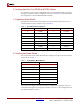
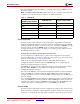
Table 6: JTAG Mode
Configuration Port User
PROM and FPGA Header
MultiLINX Pins Parallel Cable III Pins
VCC3 PWR VCC
GND GND GND
TMS TMS TMS
TDI TDI TDI
TDO RD (TDO) TDO
TCK TCK TCK