
User manual

Virtex-II Prototype Platform www.xilinx.com 25
UG015 / PN0401974 (v1.1) January 14, 2003 1-800-255-7778
Detailed Description
R
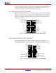
17. Clock Enable Switches 0-7
The user has access to eight additional global clocks on the DUT. These clocks can be
enabled by setting the appropriate dip switches shown in Table 10. After selecting the
clock frequency, all enabled clocks run at that frequency.
The frequency of each of these clocks can be doubled by setting the CLK_DOUBLE switch,
shown in Table 11. Clock doubling is achieved by the DLL in the Service FPGA. However,
setting this switch doubles the frequency of all enabled clocks.
The remaining four FPGA global clocks are accessible through the header pins
surrounding the DUT.
Note:
1. When LED 7 is lighted before configuration, it implies that the DLL is locked.
2. The above 12 global clocks are not available through the breakout area test points.
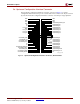
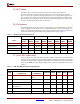
18. Clock Enable Switches 8-12
The remaining four clock enable switches are described in Table 11.
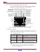
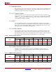
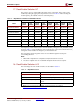
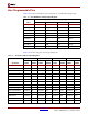
Table 10: Dip Switches and Associated Global Clocks
FG256 FG456 FG676 FF1152
Label
Clock
Name
Pin
Number
Clock
Name
Pin
Number
Clock
Name
Pin
Number
Clock
Name
Pin
Number
CLOCK ENABLE 0 GCLK1S R9 GCLK1S AA12 GCLK1S AC14 GCLK6P AK19
CLOCK ENABLE 1 GCLK6P R8 GCLK6P Y11 GCLK6P AB13 GCLK1S AK16
CLOCK ENABLE 2 GCLK5S P8 GCLK5S W11 GCLK5S AA13 GCLK2P AG17
CLOCK ENABLE 3 GCLK4P N8 GCLK4P V11 GCLK4P Y13 GCLK3S AF17
CLOCK ENABLE 4 GCLK7P D8 GCLK7P D11 GCLK7P F13 GCLK0S H16
CLOCK ENABLE 5 GCLK6S C8 GCLK6S C11 GCLK6S E13 GCLK1P H17
CLOCK ENABLE 6 GCLK5P B8 GCLK5P B11 GCLK5P D13 GCLK2S E16
CLOCK ENABLE 7 GCLK2S B9 GCLK2S F13 GCLK2S H15 GCLK5P E19
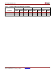
Table 11: Dip Switches 8-12
Label Function
CLK_DOUBLE Doubles the frequency of all enabled clocks
HSWAP_EN Controls user I/O pullups before configuration
DOWNSTREAM_TDO_TERM Connects TDO of last device back to the feedback
chain
(not used)
Note:
For more information about HSWAP, see the Xilinx Data Book available at:
http://www.xilinx.com/partinfo/databook.htm.