
user manual


MicroBlaze Processor Reference Guide www.xilinx.com 45
UG081 (v6.0) June 1, 2006 1-800-255-7778
R
Chapter 2
MicroBlaze Signal Interface Description
Overview
The MicroBlaze core is organized as a Harvard architecture with separate bus interface
unitsfordata accesses andinstructionaccesses.The following threememory interfacesare
supported: Local Memory Bus (LMB), IBM’s On-chip Peripheral Bus (OPB), and Xilinx
CacheLink (XCL). The LMB provides single-cycle access to on-chip dual-port block RAM.
The OPB interface provides a connection to both on-chip and off-chip peripherals and
memory. The CacheLink interface is intended for use with specialized external memory
controllers.MicroBlaze also supportsup to 8 Fast SimplexLink (FSL) ports, each withone
master and one slave FSL interface.
Features
The MicroBlaze can be configured with the following bus interfaces:
• A 32-bit version of the OPB V2.0 bus interface (see IBM’s 64-Bit On-Chip Peripheral
Bus, Architectural Specifications, Version 2.0)
• LMB provides simple synchronous protocol for efficient block RAM transfers
• FSL provides a fast non-arbitrated streaming communication mechanism
• XCL provides a fast slave-side arbitrated streaming interface between caches and
external memory controllers
• Debug interface for use with the Microprocessor Debug Module (MDM) core
• Trace interface for performance analysis
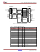
MicroBlaze I/O Overview
The core interfaces shown in Figure 2-1 and the following Table 2-1 are defined as follows:
DOPB: Data interface, On-chip Peripheral Bus
DLMB: Data interface, Local Memory Bus (BRAM only)
IOPB: Instruction interface, On-chip Peripheral Bus
ILMB: Instruction interface, Local Memory Bus (BRAM only)
MFSL 0..7: FSL master interfaces
SFSL 0..7: FSL slave interfaces
IXCL: Instruction side Xilinx CacheLink interface (FSL master/slave pair)
DXCL: Data side Xilinx CacheLink interface (FSL master/slave pair)
Core: Miscellaneous signals for: clock, reset, debug, and trace