
user manual


MicroBlaze Processor Reference Guide www.xilinx.com 55
UG081 (v6.0) June 1, 2006 1-800-255-7778
Xilinx CacheLink (XCL) Interface Description
R
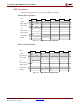
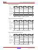
FSL Transactions
FSL BUS Write Operation
A write to the FSL bus is performed by MicroBlaze using one of the flavors of the put
instruction. A write operations transfers the register contents to an output FSL bus. The
transfer is completed in a single clock cycle for blocking mode writes to the FSL (put and
cput instructions) as long as the FSL FIFO does not become full. If the FSL FIFO is full, the
processor stalls until the FSL full flag is lowered. The non-blocking instructions: nput and
ncput, will always complete in a single clock cycle even if the FSL was full. If the FSL was
full, the write is inhibited and the carry bit is set in the MSR.
FSL BUS Read Operation
A read from the FSL bus is performed by MicroBlaze using one of the flavors of the get
instruction. A read operations transfers the contents of an input FSL to a general purpose
register.The transferis typically completed in 2 clock cycles for blockingmode reads from
the FSL (get and cgetinstructions) aslong as data exists in theFSL FIFO.If theFSL FIFO is
empty, the processor stalls at this instruction until the FSL exists flag is set. In the non-
blocking mode (nget and ncget instructions), the transfer is completed in two clock cycles
irrespective of whether or not the FSL was empty. In the case the FSL was empty, the
transfer of data does not take place and the carry bit is set in the MSR.
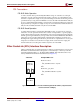
Xilinx CacheLink (XCL) Interface Description
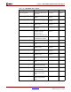
Xilinx CacheLink(XCL) is a high performance solutionfor external memory accesses. The
MicroBlaze CacheLink interface is designed to connect directly to a memory controller
with integrated FSL buffers, e.g. the MCH_OPB_SDRAM. This method has the lowest
latency and minimal number of instantiations (see Figure 2-7).
Figure 2-7: CacheLink connection with integrated FSL buffers (only Instruction
cache used in this example)
BEGIN microblaze
...
BUS_INTERFACE IXCL = myIXCL
...
END
BEGIN mch_opb_sdram
...
BUS_INTERFACE MCH0 = myIXCL
...
END
Memory
MicroBlaze
Controller
FSL
FSL
Schematic
Example MHS code