
user manual


MicroBlaze Processor Reference Guide www.xilinx.com 57
UG081 (v6.0) June 1, 2006 1-800-255-7778
Xilinx CacheLink (XCL) Interface Description
R
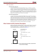
CacheLink Transactions
All individual CacheLink accesses follow the FSL FIFO based transaction protocol:
• Access information is encoded over the FSL data and control signals (e.g.
DCACHE_FSL_OUT_Data, DCACHE_FSL_OUT_Control, ICACHE_FSL_IN_Data,
and ICACHE_FSL_IN_Control)
• Information is sent (stored) by raising the write enable signal (e.g.
DCACHE_FSL_OUT_Write).
• The sender is only allowed to write if the full signal from the receiver is inactive (e.g.
DCACHE_FSL_OUT_Full = 0). The full signal is not used by the instruction cache
controller.
• Information is received (loaded) by raising the read signal (e.g.
ICACHE_FSL_IN_Read)
• The receiver is only allowed to read as long as the sender signals that new data exists
(e.g. ICACHE_FSL_IN_Exists = 1).
For details on the generic FSL protocol please refer to the “Fast Simplex Link (FSL) bus”
data sheet (DS449).
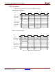
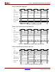
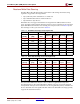
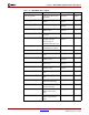
DCACHE_FSL_IN_Read Read signal to D-side
return read data FSL
std_logic output
DCACHE_FSL_IN_Data Read data from D-side
return read data FSL
std_logic_vector
(0 to 31)
input
DCACHE_FSL_IN_Control FSL control bit from D-
side return read data FSL
std_logic input
DCACHE_FSL_IN_Exists More read data exists in
D-side return FSL
std_logic input
DCACHE_FSL_OUT_Clk Clock output to D-side
read access FSL
std_logic; output
DCACHE_FSL_OUT_Write Write new cache miss
access request to D-side
read access FSL
std_logic; output
DCACHE_FSL_OUT_Data Cache miss access (read
address or write address
+ write data + byte write
enable) to D-side read
access FSL
std_logic_vector
(0 to 31)
output
DCACHE_FSL_OUT_Control FSL control-bit to D-side
read access FSL. Used
with address bits [30 to
31] for read/write and
byte enable encoding.
std_logic; output
DCACHE_FSL_OUT_Full FSL access buffer for D-
side read accesses is full
std_logic; input
Table 2-8: MicroBlaze Cache Link signals
Signal Name Description VHDL Type Direction