ML310 User Guide Virtex-II Pro Embedded Development Platform UG068 (v1.
R "Xilinx" and the Xilinx logo shown above are registered trademarks of Xilinx, Inc. Any rights not expressly granted herein are reserved. CoolRunner, RocketChips, Rocket IP, Spartan, StateBENCH, StateCAD, Virtex, XACT, XC2064, XC3090, XC4005, and XC5210 are registered trademarks of Xilinx, Inc. The shadow X shown above is a trademark of Xilinx, Inc. ACE Controller, ACE Flash, A.K.A.
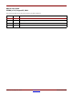
ML310 User Guide UG068 (v1.01) August 25, 2004 The following table shows the revision history for this document.. Version Revision 08/15/04 1.0 Initial Xilinx release. 08/25/04 1.01 Added SysACE CFGADDR details. UG068 (v1.01) August 25, 2004 www.xilinx.
ML310 User Guide www.xilinx.com 1-800-255-7778 UG068 (v1.
Table of Contents Preface: About This Manual Chapter 1: Introduction to Virtex-II Pro, ISE, and EDK Virtex-II Pro . . . . . . . . . . . . . . . . . . . . . . . . . . . . . . . . . . . . . . . . . . . . . . . . . . . . . . . . . . . . . . . . 11 Summary of Virtex-II Pro Features . . . . . . . . . . . . . . . . . . . . . . . . . . . . . . . . . . . . . . . . . . PowerPC™ 405 Core . . . . . . . . . . . . . . . . . . . . . . . . . . . . . . . . . . . . . . . . . . . . . . . . . . . . . . RocketIO 3.
R PCI Bus . . . . . . . . . . . . . . . . . . . . . . . . . . . . . . . . . . . . . . . . . . . . . . . . . . . . . . . . . . . . . . . . . ALi South Bridge Interface, M1535D+, U15 . . . . . . . . . . . . . . . . . . . . . . . . . . . . . . . . . . . Parallel Port Interface, connector assembly P1 . . . . . . . . . . . . . . . . . . . . . . . . . . . . . . . . Serial Port Interface, connector assembly P1 . . . . . . . . . . . . . . . . . . . . . . . . . . . . . . . . . . USB, connector assembly J3 . . . . .
R Preface About This Manual This manual accompanies the ML310 Embedded Development System and contains information about the ML310 Hardware Platform and software tools. Manual Contents This manual contains the following chapters: • Chapter 1, “Introduction to Virtex-II Pro, ISE, and EDK,” provides an overview of the hardware and software features.
R Chapter : Resource Problem Solvers Description/URL Interactive tools that allow you to troubleshoot your design issues http://support.xilinx.com/support/troubleshoot/psolvers.htm Tech Tips Latest news, design tips, and patch information for the Xilinx design environment http://www.support.xilinx.com/xlnx/xil_tt_home.jsp Conventions This document uses the following conventions. An example illustrates each convention.
R Convention Meaning or Use Example Vertical ellipsis . . . Repetitive material that has been omitted IOB #1: Name = QOUT’ IOB #2: Name = CLKIN’ . . . Horizontal ellipsis . . . Repetitive material that has been omitted allow block block_name loc1 loc2 ...
R 10 Chapter : www.xilinx.com 1-800-255-7778 ML310 User Guide UG068 (v1.
R Chapter 1 Introduction to Virtex-II Pro, ISE, and EDK Virtex-II Pro The Virtex-II Pro Platform FPGA solution is the most technically sophisticated silicon and software product development in the history of the programmable logic industry. The goal was to revolutionize system architecture “from the ground up.” To achieve that objective, the best circuit engineers and system architects from IBM, Mindspeed, and Xilinx codeveloped the world's most advanced Platform FPGA silicon product.
R Chapter 1: Introduction to Virtex-II Pro, ISE, and EDK Table 1-1: Virtex-II Pro Family Members Device 2VP2 2VP4 2VP7 2VP20 2VP30 2VP40 2VP50 2VP70 2VP100 2VP125 Logic Cells 3,168 6,768 11,088 20,880 30,816 43,632 53,136 74,448 99,216 125,136 PPC405 0 1 1 2 2 2 2 2 2 4 MGTs 4 4 8 8 8 12 16 20 20 24 BRAM (Kbits) 216 504 792 1,584 2,448 3,456 4,176 5,904 7,992 10,008 Xtreme Multipliers 12 28 44 88 136 192 232 328 444 556 PowerPC™ 405 Core •
R Virtex-II Pro • Four levels of selectable pre-emphasis • Five levels of output differential voltage • Per-channel internal loopback modes • 2.5V transceiver supply voltage Virtex-II FPGA Fabric Description of the Virtex-II Family fabric follows: • • • • SelectRAM memory hierarchy ♦ Up to 10 Mb of True Dual-Port RAM in 18 Kb block SelectRAM resources ♦ Up to 1.
R Chapter 1: Introduction to Virtex-II Pro, ISE, and EDK ♦ • • - 840 Mb/s Low-Voltage Differential Signaling I/O (LVDS) with current mode drivers - Bus LVDS I/O - HyperTransport™ (LDT) I/O with current driver buffers - Built-in DDR input and output registers Proprietary high-performance SelectLink technology for communications between Xilinx devices - High-bandwidth data path - Double Data Rate (DDR) link - Web-based HDL generation methodology SRAM-based in-system configuration ♦ Fast Se
R Foundation ISE IP. ISE even includes technology called IP Builder, which allows you to capture your own IP and reuse it in other designs. ISE’s Architecture Wizards allow easy access to device features like the Digital Clock Manager and Multi-Gigabit I/O technology. ISE also includes a tool called PACE (Pinout Area Constraint Editor) which includes a front-end pin assignment editor, a design hierarchy browser, and an area constraint editor.
R Chapter 1: Introduction to Virtex-II Pro, ISE, and EDK Board Level Integration Xilinx understands the critical issues such as complex board layout, signal integrity, highspeed bus interface, high-performance I/O bandwidth, and electromagnetic interference for system level designers.
R Chapter 2 ML310 Embedded Development Platform Overview The ML310 Embedded Development Platform offers designers a versatile Virtex-II Pro XC2VP30-FF896 based platform for rapid prototyping and system verification. In addition to the more than 30,000 logic cells, over 2,400 Kb of BRAM, dual PowerPC™ 405 processors and RocketIO transceivers available in the FPGA, the ML310 provides an onboard Ethernet MAC/PHY, DDR memory, multiple PCI bus slots, and standard PC I/O ports within an ATX form factor board.
R Chapter 2: ML310 Embedded Development Platform Figure 2-1: ML310 Board 18 www.xilinx.com 1-800-255-7778 ML310 User Guide UG068 (v1.
R Overview INTC PLB2OPB Bridge SMBus PPC 405 OCM Bus OCM BRAM XC2VP30 FF896 GPIO SPI GPIO / LEDs PCI Bridge DDR RS232 256 MB DDR DIMM 8 RocketIO MGTs 3 LVDS pairs 1 LVDS Clock pair 38 Single-Ended I/O PLB Bus UART OPB Bus High-Speed PM1 39 LVDS Pairs 1 Clock PLB BRAM OPB2PLB Bridge SMBus System ACE SPI CF SysACE Figure 2-2 shows a high-level block diagram of the ML310 and its peripherals. High-Speed PM2 3.3V PCI RJ45 Intel GD82559 10/100 Ethernet NIC AMD Flash TI PCI 2250 3.
R Chapter 2: ML310 Embedded Development Platform • ♦ 2 USB ports ♦ 2 IDE connectors ♦ GPIO ♦ SMBus Interface ♦ AC97 Audio CODEC ♦ PS/2 keyboard and mouse ports ATX power supply Board Hardware The ML310 Virtex-II Pro FPGA is connected to several peripherals listed below. The peripherals are either directly connected to the FPGA or in directly accessible via the PCI Bus.
R Board Hardware II Pro FPGA I/O can be configured to use different IO standards such as SSTL2 as required on the DDR DIMM interface. Please review the ML310 Virtex-II Pro data sheet for more information regarding I/O standards. Figure 2-3 shows the top-level clocking for the ML310 board. X8 SYACE_FPGA_CLK SYSACE X7 OSC 156.
R Chapter 2: ML310 Embedded Development Platform DDR Signaling The FPGA DDR DIMM interface supports SSTL2 signaling. All DDR signals are controlled impedance and are SSTL2 terminated. DDR Memory Expansion The FPGA is capable of replicating up to three differential clock output pairs to the DIMM in order to support either registered or unbuffered DIMMs. The ML310 DDR interface is very flexible in the event different DDR memory is desired such as an unbuffered DIMM or increased memory size.
R Board Hardware Table 2-1: Connections from FPGA to DIMM Interface, P7 UCF Signal Name XC2VP30 Pin (U37) DIMM (P7) Schem Signal Name ddr_ad[2] AG20 DDR_A2 41 ddr_ad[3] AF23 DDR_A3 130 ddr_ad[4] AH22 DDR_A4 37 ddr_ad[5] AF22 DDR_A5 32 ddr_ad[6] AF21 DDR_A6 125 ddr_ad[7] AH21 DDR_A7 29 ddr_ad[8] AG21 DDR_A8 122 ddr_ad[9] AJ21 DDR_A9 27 ddr_ad[10] AK21 DDR_A10 141 ddr_ad[11] AH20 DDR_A11 118 ddr_ad[12] AF20 DDR_A12 115 ddr_ba[0] AG18 DDR_BA0 59 ddr_ba[1]
R Chapter 2: ML310 Embedded Development Platform Table 2-1: Connections from FPGA to DIMM Interface, P7 UCF Signal Name 24 XC2VP30 Pin (U37) DIMM (P7) Schem Signal Name ddr_dqs[5] M29 DDR_DQS02 25 ddr_dqs[6] H29 DDR_DQS01 14 ddr_dqs[7] F29 DDR_DQS00 5 ddr_dq[0] AG28 DDR_DQ63 179 ddr_dq[1] AG26 DDR_DQ62 178 ddr_dq[2] AE26 DDR_DQ61 175 ddr_dq[3] AD26 DDR_DQ60 174 ddr_dq[4] AH27 DDR_DQ59 88 ddr_dq[5] AH26 DDR_DQ58 87 ddr_dq[6] AF25 DDR_DQ57 84 ddr_dq[7] AD25 D
R Board Hardware Table 2-1: Connections from FPGA to DIMM Interface, P7 UCF Signal Name XC2VP30 Pin (U37) DIMM (P7) Schem Signal Name ddr_dq[32] N27 DDR_DQ31 133 ddr_dq[33] P26 DDR_DQ30 131 ddr_dq[34] R25 DDR_DQ29 127 ddr_dq[35] R27 DDR_DQ28 126 ddr_dq[36] N28 DDR_DQ27 40 ddr_dq[37] P27 DDR_DQ26 39 ddr_dq[38] R26 DDR_DQ25 35 ddr_dq[39] R28 DDR_DQ24 33 ddr_dq[40] K27 DDR_DQ23 123 ddr_dq[41] L26 DDR_DQ22 121 ddr_dq[42] M27 DDR_DQ21 117 ddr_dq[43] N26 DDR_D
R Chapter 2: ML310 Embedded Development Platform unbuffered DIMM requires more than one clock input pair versus a single clock input pair for a registered DIMM. Table 2-2 shows optional clocking connections that are required for interfacing the FPGA to unbuffered DDR DIMMs.
R Board Hardware a UART usable with any member of the Virtex-II Pro device family. Please review the EDK Processor IP Reference Guide for more details. The RS-232 port directly connected to the XC2VP30 is accessible by a 10 pin header(J4). An RS-232 mini-cable adapter included with the ML310 converts J4, 10 pin header, to a DB9 male connector. The adapter is a standard DTK/Intel IDC-10 to DB9 Male.
R Chapter 2: ML310 Embedded Development Platform Non-Volatile Storage In addition to programming the FPGA and storing bitstreams, System ACE can be used for general use non-volatile storage. System ACE provides an MPU interface for allowing a microprocessor to access the CompactFlash, allowing the use of the CompactFlash as a file system.
R Board Hardware JTAG JTAG is a simple interface that provides for many uses. On the ML310 Hardware Platform, the primary uses include configuration of the XC2VP30, debugging software (similar to the CPU debug interface), and debugging hardware using the ChipScope™ Integrated Logic Analyzer (ILA). The Virtex-II Pro family is fully compliant with the IEEE Standard 1149.1 Test Access Port and Boundary-Scan Architecture. The architecture includes all mandatory elements defined in the IEEE 1149.1 Standard.
R Chapter 2: ML310 Embedded Development Platform Parallel Cable IV Interface The Parallel Cable IV (PC IV) download cable can also be used to program the XC2VP30. The pinout provided in Figure 2-7 is compatible with the PC IV JTAG programming solution. Figure 2-7 shows the pinout of the PC IV JTAG connector.
R Board Hardware VCC3V3 U36 20 DBG_LED_0 DBG_LED_1 DBG_LED_2 DBG_LED_3 19 11 13 15 17 R399 1OE 1A1 1A2 1A3 1A4 2OE 2A1 2A2 2A3 2A4 4.
R Chapter 2: ML310 Embedded Development Platform GPIO LED Interface All LEDs connected to the GPIO lines illuminate Green when driven with a logic zero and extinguish with a logic one. Table 2-6 shows the connections for the GPIO LEDs from the FPGA to the non-inverting buffer (U36).
R Board Hardware The three GPIO signals configured as outputs only are used as control signals that allows the user to read/write the LCD character display in conjunction with the eight LCD data signals defined earlier in Table 2-7. Please review the AND491GST LCD display data sheet located on the ML310 CDROM for more detailed information. Table 2-8 shows the control signal connections for the GPIO LCD from the FPGA to U33.
R Chapter 2: ML310 Embedded Development Platform The PPC405 JTAG (Joint Test Action Group) Debug port complies with IEEE standard 1149.1-1990, IEEE Standard Test Access Port and Boundary Scan Architecture. This standard describes a method for accessing internal chip resources using a four-signal or five-signal interface. The PPC405 JTAG Debug port supports scan-based board testing and is further enhanced to support the attachment of debug tools. These enhancements comply with the IEEE 1149.
R Board Hardware CPU Debug Connector Pinout Figure 2-10 shows J12, the 16 pin header used to debug the operation of software in the CPU. This is done using debug tools such as Parallel Cable IV or third party tools. Refer to the PPC405 Processor Block Manual for more information on the JTAG debug-port signals.
R Chapter 2: ML310 Embedded Development Platform Arbiter IP. Please see the EDK Processor IP Reference Guide for more information about the EDK IP mentioned in this section. The FPGA is responsible generating the PCI RST signal as well as the PCI CLK signal. The FPGA fabric is used to generate six PCI Clocks that drive each of the PCI devices/slots shown in the Figure 2-11. All six PCI Clock outputs are length matched.
R Board Hardware 3.3V PCI-to-PCI 5.0V Bridge TI2250 U32 5.0V PCI Slot 6 PCI_S_CLK0 PCI_S_AD18 IDSEL PCI_BUS 5.0V PCI Slot 4 PCI_S_CLK1 U37 PCI_S_AD19 IDSEL PCI_BUS 0xAC23 104C IDSEL PCI Bus Virtex-II Pro FPGA XC2VP30 PCI_P_AD24 PCI_P_AD25 IDSEL PCI_BUS PCI_P_CLK5 PCI_P_CLK4 PCI_P_CLK0 PCI_P_CLK1 PCI_P_CLK2 PCI_P_CLK3 3.3V PCI Slot 5 PCI_P_AD21 PCI_P_AD22 IDSEL PCI_BUS 3.
R Chapter 2: ML310 Embedded Development Platform Table 2-10: PCI Controller Connections (Continued) UCF Signal Name XC2VP30 Pin (U37) Description PCI_INTA L5 PCI_INTB N2 PCI_INTC M2 PCI_INTD R9 PCI_INTE P9 PCI_INTF M3 PCI_REQ0_N P1 PCI_REQ1_N N1 PCI_REQ2_N P7 PCI_REQ3_N P8 PCI_REQ4_N N3 PCI_GNT0_N P2 PCI_GNT1_N P3 PCI_GNT2_N R7 PCI_GNT3_N R8 PCI_GNT4_N P4 PCI_CBE[0] J2 PCI_CBE[1] H2 PCI_CBE[2] M7 PCI_CBE[3] M8 PCI_FRAME_N K6 PCI_IRDY_N K1 PCI_TRDY_N J1 PC
R Board Hardware Table 2-10: PCI Controller Connections (Continued) UCF Signal Name XC2VP30 Pin (U37) Description PCI_AD[0] G5 PCI_AD[1] G6 PCI_AD[2] D5 PCI_AD[3] C5 PCI_AD[4] C1 PCI_AD[5] C2 PCI_AD[6] J7 PCI_AD[7] J8 PCI_AD[8] D3 PCI_AD[9] C4 PCI_AD[10] D1 PCI_AD[11] D2 PCI_AD[12] H5 PCI_AD[13] H6 PCI_AD[14] E3 PCI_AD[15] E4 PCI_AD[16] E1 PCI_AD[17] E2 PCI_AD[18] K7 PCI_AD[19] K8 PCI_AD[20] F3 PCI_AD[21] F4 PCI_AD[22] F1 PCI_AD[23] F2 PCI_AD[24] J5 P
R Chapter 2: ML310 Embedded Development Platform Table 2-11 describes how the Primary PCI Bus interrupts are connected on the ML310 board along with each devices IDSEL, REQ/GNT, PCI Clocks and DeviceID/Vendor ID information. Table 2-11: 3.
R Board Hardware ALi M1535D+ supports the following features: ♦ 1 parallel and 2 serial ports ♦ 2 USB ports ♦ 2 IDE connectors ♦ GPIO ♦ SMBus Interface ♦ AC97 Audio CODEC ♦ PS/2 keyboard and mouse U37 IDSEL PCI_P_AD24 U15 PCI_BUS PCI_P_CLK3 X4 OSC 32.768 MHz ALi South Bridge FPGA X2 OSC 48MHz PCI_P_AD17 PCI_P_AD18 PCI_P_AD19 PCI_P_AD26 PCI_P_AD27 PCI_P_AD31 IDSEL Device ID Vendor ID Audio 0x5451 0x10B9 S.
R Chapter 2: ML310 Embedded Development Platform Table 2-13 shows the ALi Parallel Port connections to P1, DB25. Table 2-13: ALi South Bridge Parallel Port pinout P1 (DB25) Signal Name P1 (DB25) Pin No.
R Board Hardware Table 2-14 shows the RS-232 signals connected to the two DB9 connectors, P1 A/B. Table 2-14: ALi South Bridge DB9 Serial Port pinouts, P1 (DB9-A/B) Signal Name P1 (DB9-A/B) Pin No. Description DCD 1 Data Carrier Detect RD 2 Receive Data (a.k.a RxD, Rx) TD 3 Transmit Data (a.k.
R Chapter 2: ML310 Embedded Development Platform IDE, connectors J15 and J16 Supports a 2-channel UltraDMA-133 IDE Master controller independently connected to a Primary 40 Pin IDC connector (J16) and a Secondary 40 Pin IDC connector (J15). Please review the ALi M1535D+ Data sheets for more detailed information. Table 2-16 shows the ALi Primary and Secondary IDE connections to the two 40 pin IDE Connectors, J15 and J16. Table 2-16: J15/J16 Pin No.
R Board Hardware GPIO, connector J5 There are 15 GPIO pins connecting the ALi M1535D+ to the J5 24 pin header. These may be accessed via the ALi M1535D+ via the PCI Bus. Please review the ALi M1535D+ Data sheets for more detailed information. Table 2-17 shows the types and number of GPIO signals available to the user from the ALi South Bridge.
R Chapter 2: ML310 Embedded Development Platform send byte/receive byte/ write byte/write word/read word/block read/block write command with clock synchronization function as well as 10-bit addressing ability. Please see Section “IIC/SMBus Interface” for more information regarding the devices that are connected to the SMBus. Please review the ALi M1535D+ Data sheets for more detailed information. AC97 Audio The ALi South Bridge has a built-in Audio that is combined with a standard AC97 CODEC, LM4550.
R Board Hardware PS/2 Keyboard/Mouse Interface, connector P2 The ALi M1535D+ has a built-in PS2/AT Keyboard and PS/2 Mouse controller. The PS/2 Keyboard and Mouse ports are connected to the ALi M1535D+ via standard DIN connectors contained in the P2 connector assembly. In the event of a short circuit by the keyboard or mouse device, the 5V power provided to these devices is fuse protected by a resettable fuse, F1. Please review the ALi M1535D+ Data sheets for more detailed information.
R Chapter 2: ML310 Embedded Development Platform Table 2-21: ALi M1535 Flash Memory Interface Schem Net Name M1535D+ (U15) AM29F040B (U4) ROM_A18 T15 9 ROM_A17 U15 6 ROM_A16 V15 10 ROM_A15 W15 11 ROM_A14 T16 5 ROM_A13 U16 4 ROM_A12 V16 12 ROM_A11 W16 1 ROM_A10 Y16 31 ROM_A9 R17 2 ROM_A8 T17 3 ROM_A7 U17 13 ROM_A6 V17 14 ROM_A5 W17 15 ROM_A4 Y17 16 ROM_A3 V18 17 ROM_A2 W18 18 ROM_A1 Y18 19 ROM_A0 V19 20 Description Flash Addresses Intel GD8255
R Board Hardware review the GD82559 Data sheet, located on the ML310 CDROM, for more detailed information. U37 U11 INTEL GD82559 Ethernet MAC/PHY PCI_P_CLK2 FPGA XC2VP30 X5 OSC 25MHz Vendor ID 0x8086 Device ID 0x1229 PCI_P_AD23 PCI_BUS IDSEL PCI_BUS Figure 2-13: J3 RJ45 U16 EEPROM Intel GD82559 Ethernet Controller IIC/SMBus Interface Introduction to IIC/SMBus The Inter Integrated Circuit (IIC) bus provides the connection from the CPU to peripherals.
R Chapter 2: ML310 Embedded Development Platform Table 2-22 shows the FPGA connections to all SMBus and IIC devices. Table 2-22: SMBus and IIC Controller Connections UCF Signal Name XC2VP30 Pin Schem Signal Name iic_scl C13 fpga_scl iic_sda J15 fpga_sda iic_irq_n E15 iic_irq_n iic_temp_crit_n* D15 iic_therm_n * Note: This signal connects to U20 therm_l on the LM87. See data sheet for additional details. 50 www.xilinx.com 1-800-255-7778 ML310 User Guide UG068 (v1.
R Board Hardware Table 2-14 shows a block diagram of the FPGA in relation to the SMBus accelerator and the IIC bus.
R Chapter 2: ML310 Embedded Development Platform Table 2-23 lists the IIC devices and their associated addresses. Table 2-23: IIC Devices and Addresses Reference Designator Address LTC1694 U27 n/a SMBus accelerator that ensures data integrity with multiple devices on the SMBus. Enhances data transmission speed and reliability under all specified SMBus loading conditions and is compatible with the IIC bus.
R Board Hardware SPI Addressing The SPI does not use an addressed based system like the IIC Bus Interface uses. Instead, devices are selected by dedicated Slave Select signals, comparable to a Chip Select signal. Each SPI Slave device needs its own Slave Select signal driven from the SPI master. This increases the total pin count, but decreases overhead and complexity, which increases the available bandwidth and decreases bus contention.
R Chapter 2: ML310 Embedded Development Platform CPU Reset, SW2 SW2 provides a way to manually reset the powerpc system implemented in the XC2VP30. The user is responsible for connecting this signal to the PPC405 system implemented in the FPGA fabric. The EDK kit provides IP to perform this task, please review the EDK Processor IP reference Guide for more details. When SW2 is actuated it drives the signal PB_FPGA_CPU_RESET low which causes the LTC1326 (U30) to generate a 100us active low pulse.
R Board Hardware SW3 = 0 0 0 (default) 2.5V System ACE U38 2 0 1 1 2 3 ON Shown here with CFGADDR[2:0] set to "000". ON => SW Closed SYSACE CFG CFGADDR SW3 RESET SYSACE_ RESET_N CFGADDR[2:0] = SW1 U31 Debounce SYSACE Reset 0x0 Default 0x1 0x2 0x3 0x4 0x5 0x6 0x7 Figure 2-16: SW3 - SysACE CFG Switch Detail Front Panel Interface Connector, J23 The Front panel Interface connector (J23) is a 24-pin header that accepts a standard IDC 24 pin connector (0.1inch pitch).
R Chapter 2: ML310 Embedded Development Platform The front panel interface provides the following status information available at the J23 header.
R Board Hardware Table 2-25: J23 Pin Front Panel Interface connector, J23 Schem Signal Description 15 KBINH Tie this pin to GND to activate Keyboard inhibit, see ALi M1536D+ data sheet for more details 16 VCC5V 5V ATX power available to user 17 ATX_IDELED_R ATX IDE access indicator, Tie this pin to Anode of user’s LED and Cathode to GND 18 VCC5V 5V ATX power available to user 19 PWR_SUPPLY_ON Short this pin to GND to enable the ATX power supply.
R Chapter 2: ML310 Embedded Development Platform MGT BREF Clock Selection Jumpers, J20 and J21 One of two onboard LVDS BREF clock sources, X7 or X9, can be selected via jumpers, J20 and J21. The selected clock source drives both top and bottom LVDS BREF Clock input pairs to the XC2VP30 FPGA. Table 2-27 shows the MGT BREF clock selections available on the ML310 board. Table 2-27: Jumper Selection for MGT BREF clocks,J20/J21 Jumper (J10) Jumper (J11) 156.
R Board Hardware Note: An Antec, model SL250S, ATX Power Supply is delivered with your ML310. The Antec User’s Manual is provided in the Data sheets section on the ML310 CDROM. Prior to installation please read the Installation section of the Antec User’s Manual which describes the red voltage switch power setting on your Antec SL250S supply. Check the red power supply voltage switch setting before installation. It should be the same as your local power voltage (115V for North America, Japan, etc.
R Chapter 2: ML310 Embedded Development Platform In addition to the MC34161D voltage monitors, the ML310 employs a SMBus device, LM87, which samples several of the same supply voltages when accessed over the System Management Bus or SMBus. More information on the SMBus features of the ML310 can be found in section “IIC/SMBus Interface”. VCC1V5 VCC5V VCC5V 1.5V 5.0V U29 MC34161D VCC2V5 RED = Fault GRN = Nominal GRN = Nominal MC34161D DS8 VCC5V VTT_DDR DS7 VCC5V TP13 2.
R High-Speed I/O Table 2-28 Shows the various Voltage monitor information. Table 2-28: Voltage Monitor Information Schem Name Voltage Testpoint *Indicator LED Notes VCC1V5 1.5V TP17 DS8 Regulated FPGA Core voltage VCC2V5 2.5V TP14 DS6 Regulated FPGA / Board Logic VCC3_PCI 3.0V TP10 DS4 Regulated FPGA PCI Bank 1-2 Voltage VCC3V3 3.3V TP8 DS2 Regulated PCI/Misc Logic VCC5V 5.0V TP16 DS7 From ATX Supply, All Regulators Derive Power VTT_DDR 1.
R Chapter 2: ML310 Embedded Development Platform PM1 Adapter Board Connector Host Board Connector PM2 Personality Module Figure 2-19: ML310 Board Personality Module Connected to ML310 Board ML310 PM Connectors The ML310 PM connectors are Tyco Z-Dok+ connectors, part number 1367550-5. The "-5" suffix indicates a 40 pair connector. Each connector has 40 differential pairs and several power and ground pins.
R High-Speed I/O Figure 2-20 shows an edge view of the PM host board connectors on the ML310 board. PM1 Host Board Connector PM2 Host Board Connector Figure 2-20: Edge View of Host Board Connectors on ML310 Each signal pair on the PM1 and PM2 host board connectors has a wide ground pin on the opposite side of the plastic divider, as shown in Figure 2-21. The signal pairs alternate from side to side along the length of the divider. All of the "B" and "E" pins are grounded on the ML310.
R Chapter 2: ML310 Embedded Development Platform • 1 single-ended clock at 2.5V • 1 pin not connected Adapter Board PM Connectors Tyco Z-Dok+ adapter board connectors, part number 1367555-1 are the receptacle connectors on the personality modules that mate to the ML310 Tyco Z-Dok+ host board connectors, part number 1367550-5. The Tyco data sheet for part number 1367555-1 is available at http://www.z-dok.com/documents/1367555.pdf.
R High-Speed I/O PM1 Power and Ground Table 2-29 shows the power and ground pins for the PM1 connector on the ML310. Table 2-29: PM1 Power and Ground Pins Pin Number Description Length Contact Order 1, 6 Ground Level 4 First 2, 5 2.5V Level 3 Second 3 3.3V Level 2 Third 4 1.5V Level 2 Third PM2 Power and Ground Table 2-30 shows the power and ground pins for the PM2 connector on the ML310.
R Chapter 2: ML310 Embedded Development Platform Table 2-31: PM1 Pin 66 PM1 Pinout (Continued) FPGA Pin Pin Description ML310 Schematic Net FPGA Bank VCCO A11 H16 IO_L69P_0 PM_IO_82 2.5V A12 J16 IO_L69N_0 PM_IO_83 2.
R High-Speed I/O Table 2-31: PM1 Pin PM1 Pinout (Continued) FPGA Pin Pin Description ML310 Schematic Net FPGA Bank VCCO D4 G25 IO_L02N_7 PM_IO_85 D5 A8 IO_L44N_1 PM_IO_3V_21 3V D6 B8 IO_L44P_1 PM_IO_3V_20 3V D7 D7 IO_L08P_1 PM_IO_3V_8 3V D8 F9 IO_L07P_1 PM_IO_3V_6 3V D9 E8 IO_L03P_1 PM_IO_3V_2 3V D10 D8 IO_L38P_1 PM_IO_3V_14 3V D11 D17 IO_L67P_0 PM_IO_78 2.5V D12 E17 IO_L67N_0 PM_IO_79 2.
R Chapter 2: ML310 Embedded Development Platform Table 2-31: PM1 Pin PM1 Pinout (Continued) FPGA Pin Pin Description ML310 Schematic Net F17 AK11 RXNPAD18 RXNPAD18_AK11 F18 AK12 RXPPAD18 RXPPAD18_AK12 F19 AK24 RXNPAD21 RXNPAD21_AK24 F20 AK25 RXPPAD21 RXPPAD21_AK25 FPGA Bank VCCO Notes: 1. LVDS pairs are shown shaded; all other signals are single-ended. 2. LVDS pairs can also be used as single-ended I/O at 2.5V 3. NC indicates a “no connect” signal.
R High-Speed I/O Table 2-32: PM2 Pin PM2 Pinout (Continued) FPGA Pin Pin Description ML310 Schematic Net FPGA Bank VCCO C1 W1 IO_L57N_3 PM_IO_53 2.5V C2 Y1 IO_L57P_3 PM_IO_52 2.5V C3 U4 IO_L85N_3 PM_IO_61 2.5V C4 U5 IO_L85P_3 PM_IO_60 2.5V C5 W5 IO_L50N_3 PM_IO_39 2.5V C6 W6 IO_L50P_3 PM_IO_38 2.5V C7 V5 IO_L55N_3 PM_IO_49 2.5V C8 V6 IO_L55P_3 PM_IO_48 2.5V C9 AE14 IO_L68P_4 PM_IO_74 2.5V C10 AD14 IO_L68N_4 PM_IO_75 2.
R Chapter 2: ML310 Embedded Development Platform Table 2-32: PM2 Pin PM2 Pinout (Continued) FPGA Pin Pin Description ML310 Schematic Net FPGA Bank VCCO D14 AA5 IO_L44N_3 PM_IO_27 2.5V D15 AC4 IO_L43P_3 PM_IO_24 2.5V D16 AC3 IO_L43N_3 PM_IO_25 2.5V D17 AE4 IO_L33P_3 PM_IO_10 2.5V D18 AE3 IO_L33N_3 PM_IO_11 2.5V D19 AF4 IO_L34P_3 PM_IO_12 2.5V D20 AF3 IO_L34N_3 PM_IO_13 2.5V F1 AA1 IO_L51N_3 PM_IO_41 2.5V F2 AB1 IO_L51P_3 PM_IO_40 2.