SP605 Hardware User Guide [Guide Subtitle] [optional] UG526 (v1.1.
Xilinx is disclosing this user guide, manual, release note, and/or specification (the "Documentation") to you solely for use in the development of designs to operate with Xilinx hardware devices. You may not reproduce, distribute, republish, download, display, post, or transmit the Documentation in any form or by any means including, but not limited to, electronic, mechanical, photocopying, recording, or otherwise, without the prior written consent of Xilinx.
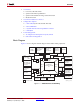
Table of Contents Preface: About This Guide Guide Contents . . . . . . . . . . . . . . . . . . . . . . . . . . . . . . . . . . . . . . . . . . . . . . . . . . . . . . . . . . . . . . 5 Additional Documentation . . . . . . . . . . . . . . . . . . . . . . . . . . . . . . . . . . . . . . . . . . . . . . . . . . . 5 Additional Support Resources . . . . . . . . . . . . . . . . . . . . . . . . . . . . . . . . . . . . . . . . . . . . . . . . 6 Chapter 1: SP605 Evaluation Board Overview . . . . . . . . . . . . . .
System ACE CF CompactFlash Image Select DIP Switch S1 (Active-High) . . . . . . . . . . 48 Mode DIP Switch SW1 (Active-High) . . . . . . . . . . . . . . . . . . . . . . . . . . . . . . . . . . . . . . . 49 18. VITA 57.1 FMC LPC Connector . . . . . . . . . . . . . . . . . . . . . . . . . . . . . . . . . . . . . . . . . . 50 Power Management . . . . . . . . . . . . . . . . . . . . . . . . . . . . . . . . . . . . . . . . . . . . . . . . . . . . . . . . . 52 AC Adapter and 12V Input Power Jack/Switch . . . .
Preface About This Guide This manual accompanies the Spartan®-6 FPGA SP605 Evaluation Board and contains information about the SP605 hardware and software tools. Guide Contents This manual contains the following chapters: • Chapter 1, “SP605 Evaluation Board,” provides an overview of the embedded development board and details the components and features of the SP605 board. • Appendix A, “Default Jumper and Switch Settings.” • Appendix B, “VITA 57.1 FMC LPC Connector Pinout.
Preface: About This Guide This guide describes the clocking resources available in all Spartan-6 devices, including the DCMs and PLLs. • Spartan-6 FPGA Block RAM Resources User Guide This guide describes the Spartan-6 device block RAM capabilities. • Spartan-6 FPGA GTP Transceivers User Guide This guide describes the GTP transceivers available in the Spartan-6 LXT FPGAs.
Chapter 1 SP605 Evaluation Board Overview The SP605 board enables hardware and software developers to create or evaluate designs targeting the Spartan®-6 XC6SLX45T-3FGG484 FPGA. The SP605 provides board features common to many embedded processing systems. Some commonly used features include: a DDR3 component memory, a 1-lane PCI Express® interface, a tri-mode Ethernet PHY, general purpose I/O and a UART.
Chapter 1: SP605 Evaluation Board Features The SP605 board provides the following features: • 1. Spartan-6 XC6SLX45T-3FGG484 FPGA • 2. 128 MB DDR3 Component Memory • 3. SPI x4 Flash • 4. Linear BPI Flash • 5. System ACE CF and CompactFlash Connector • 6. USB JTAG • 7. Clock Generation • • ♦ Fixed 200 MHz oscillator (differential) ♦ Socket with a 2.5V 27MHz oscillator (single-ended) ♦ SMA connectors (differential) ♦ SMA connectors for MGT clocking (differential) 8.
Overview • 17. Switches ♦ Power On/Off slide switch ♦ System ACE CF Reset pushbutton ♦ System ACE CF bitstream image select DIP switch ♦ Mode DIP switch • 18. VITA 57.1 FMC LPC Connector • Configuration Options • ♦ 3. SPI x4 Flash (both onboard and off-board) ♦ 4. Linear BPI Flash ♦ 5. System ACE CF and CompactFlash Connector ♦ 6.
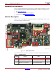
Chapter 1: SP605 Evaluation Board Related Xilinx Documents Prior to using the SP605 Evaluation Board, users should be familiar with Xilinx resources. See the following locations for additional documentation on Xilinx tools and solutions: • ISE: www.xilinx.com/ise • Answer Browser: www.xilinx.com/support • Intellectual Property: www.xilinx.com/ipcenter Detailed Description Figure 1-2 shows a board photo with numbered features corresponding to Table 1-1 and the section headings in this document.
Detailed Description Table 1-1: SP605 Features (Cont’d) Number Feature Notes Schematic Page 4 Linear BPI Flash x16 Numonyx JS28F256P30T95 19 5 SystemACE CompactFlash Socket XCCACE-TQ144I Controller 20 6 USB JTAG Conn. (USB Mini-B) USB JTAG Download Circuit 32 Clock Generation 200 MHz OSC, oscillator socket, SMA connectors 7 13, 14 a. 200 MHz oscillator Epson 200 MHz 2.5V LVDS 14 b. Oscillator socket, singleended, LVCMOS MMD Components 2.5V 27 MHz 14 c.
Chapter 1: SP605 Evaluation Board Table 1-1: SP605 Features (Cont’d) Number Feature Power, Configuration, Pushbutton Switches Switches 17 18 Schematic Page 14, 18, 20, 25 a. SP605 Power On-Off Slide Switch 25 b. FPGA Mode DIP Switch 18 c. System ACE CF Configuration DIP Switch 20 d. FPGA PROG, CPU Reset, and System ACE CF Reset Pushbutton Switches 14, 20 FMC LPC Connector 19 Notes Samtec ASP-134603-01 a. Power Management Controller 2x TI UCD9240PFC b.
Detailed Description I/O Voltage Rails There are four available banks on the XC6SLX45T-3FGG484 device. Banks 0, 1, and 2 are connected for 2.5V I/O. Bank 3 is used for the 1.5V DDR3 component memory interface of Spartan-6 FPGA’s hard memory controller. The voltage applied to the FPGA I/O banks used by the SP605 board is summarized in Table 1-2. Table 1-2: I/O Voltage Rail of FPGA Banks FPGA Bank I/O Voltage Rail 0 2.5V 1 2.5V 2 2.5V 3 1.
Chapter 1: SP605 Evaluation Board Table 1-4: FPGA On-Chip (OCT) Termination External Resistor Requirements U1 FPGA Pin FPGA Pin Number Board Connection for OCT ZIO P3 No Connect RZQ L6 100 ohms to GROUND Table 1-5 shows the connections and pin numbers for the DDR3 Component Memory.
Detailed Description Table 1-5: DDR3 Component Memory Connections (Cont’d) Memory U42 U1 FPGA Pin Schematic Net Name T1 Pin Number Pin Name MEM1_DQ9 C3 DQ9 U3 MEM1_DQ10 A2 DQ13 U1 MEM1_DQ11 D7 DQ8 W3 MEM1_DQ12 A3 DQ15 W1 MEM1_DQ13 C8 DQ10 Y2 MEM1_DQ14 B8 DQ14 Y1 MEM1_DQ15 A7 DQ12 H2 MEM1_WE_B L3 WE_B M5 MEM1_RAS_B J3 RAS_B M4 MEM1_CAS_B K3 CAS_B L6 MEM1_ODT K1 ODT K4 MEM1_CLK_P J7 CLK_P K3 MEM1_CLK_N K7 CLK_N F2 MEM1_CKE K9 CKE N3 MEM1_LDQS_P
Chapter 1: SP605 Evaluation Board 3. SPI x4 Flash The Xilinx Spartan-6 FPGA hosts a SPI interface which is visible to the Xilinx iMPACT configuration tool. The SPI memory device operates at 3.0V; the Spartan-6 FPGA I/Os are 3.3V tolerant and provide electrically compatible logic levels to directly access the SPI flash through a 2.5V bank. The XC6SLX45T-3FGG484 is a master device when accessing an external SPI flash memory device.
Detailed Description Table 1-6: SPI x4 Memory Connections SPI MEM U32 U1 FPGA Pin Schematic Net Name AB2 SPI HDR J17 Pin # Pin Name Pin # Pin Name FPGA_PROG_B – – 1 – T14 FPGA_D2_MISO3 1 IO3_HOLD_B 2 – R13 FPGA_D1_MISO2_R 9 IO2_WP_B 3 – AA3 SPI_CS_B – – 4 TMS AB20 FPGA_MOSI_CSI_B_MISO0 15 DIN 5 TDI AA20 FPGA_D0_DIN_MISO_MISO1 8 IO1_DOUT 6 TDO Y20 FPGA_CCLK 16 CLK 7 TCK – – – – 8 GND – – – – 9 VCC3V3 J46.
Chapter 1: SP605 Evaluation Board 4. Linear BPI Flash A Numonyx JS28F256P30 Linear Flash memory (U25) on the SP605 (Figure 1-5) provides 32 MB of non-volatile storage that can be used for configuration as well as software storage. The Linear Flash is operated in asynchronous mode. For details on configuring the FPGA, see “Configuration Options.
Detailed Description Table 1-7: Linear Flash Connections (Cont’d) U25 BPI FLASH U1 FPGA Pin SP605 Hardware User Guide UG526 (v1.1.
Chapter 1: SP605 Evaluation Board FPGA Design Considerations for the Configuration Flash The SP605 has the P30 BPI flash connected to the FPGA dual use configuration pins and is not shared. It can be used to configure the FPGA, and then controlled post-configuration via the FPGA fabric. After FPGA configuration, the FPGA design can disable the configuration flash or access the configuration flash to read/write code or data.
Detailed Description System ACE CF error and status LEDs indicate the operational state of the System ACE CF controller: • A blinking red error LED indicates that no CompactFlash card is present • A solid red error LED indicates an error condition during configuration • A blinking green status LED indicates a configuration operation is ongoing • A solid green status LED indicates a successful download The mode SW1 setting is important because the System ACE CF can fail to configure the FPGA when th
Chapter 1: SP605 Evaluation Board Table 1-8: System ACE CF Connections (Cont’d) U1 FPGA Pin U17 XCCACETQ144I Schematic Net Name(1) Pin Number Pin Name AA1 SYSACE_MPBRDY 39 MPBRDY W4 SYSACE_MPCE 42 MPCE AA2 SYSACE_MPIRQ 41 MPIRQ T6 SYSACE_MPOE 77 MPOE T5 SYSACE_MPWE 76 MPWE G17 SYSACE_CFGTDI 81 CFGTDI A21 FPGA_TCK 80 CFGTCK E18 FPGA_TDI 82 CFGTDO D20 FPGA_TMS 85 CFGTMS N19 CLK_33MHZ_SYSACE(2) 93 CLK Notes: 1. U17 System ACE CF controller 3.
Detailed Description FMC bypass jumper J19 must be connected between pins 1-2 (bypass) to enable JTAG access to the FPGA on the basic SP605 board (without FMC expansion modules installed), as shown in Figure 1-7. When the VITA 57.1 FMC LPC expansion connector is populated with an expansion module that has a JTAG chain, jumper J19 must be set to connect pins 2-3 in order to include the FMC expansion module's JTAG chain in the main SP605 JTAG chain.
Chapter 1: SP605 Evaluation Board Oscillator Socket (Single-Ended, 2.5V or 3.3V) One populated single-ended clock socket (X2) is provided for user applications. The option of 2.5V or 3.3V power may be selected via a 0 ohm resistor selection. The SP605 board is shipped with a 27 MHz 2.5V oscillator installed. Figure 1-8 shows the unpopulated user oscillator socket. This figure indicates the socket pin 1 location. Figure 1-9 shows the oscillator installed, with its pin 1 location identifiers.
Detailed Description SMA Connectors (Differential) A high-precision clock signal can be provided to the FPGA using differential clock signals through the onboard 50-ohm SMA connectors J38 (N) and J41 (P). Table 1-9: SP605 Clock Source Connections U1 FPGA Pin Schematic Net Name Pin Number Pin Name K22 SYSCLK_N 5 OUT_B K21 SYSCLK_P 4 OUT X2 27MHZ OSC AB13 USER_CLOCK 5 OUT USER_SMA_CLOCK M19 USER_SMA_CLOCK_N J38.1 – SMA Connectors M20 USER_SMA_CLOCK_P J41.
Chapter 1: SP605 Evaluation Board 2 SMA_RX_C_N J35 32K10K-400E3 GND1 2 GND2 3 GND3 4 1 SIG GND4 5 GND5 6 GND6 7 GND7 8 SMA_RX_C_P J34 32K10K-400E3 GND1 2 GND2 3 GND3 4 1 SIG GND4 5 GND5 6 GND6 7 GND7 8 C33 0.1UF 10V X5R 1 X-Ref Target - Figure 1-10 2 C34 0.1UF 10V X5R 1 SMA_RX_N SMA_RX_P SMA MGT Connectors J33 32K10K-400E3 GND1 2 GND2 3 GND3 4 1 SIG GND4 5 GND5 6 GND6 7 GND7 8 SMA_TX_N SMA_TX_P J32 32K10K-400E3 GND1 2 GND2 3 GND3 4 1 SIG GND4 5 GND5 6 GND6 7 GND7 8 2 C35 0.
Detailed Description Table 1-10: GTP SMA Clock Connections U1 FPGA Pin Schematic Net Name SMA Pin C9 SMA_RX_N J35.1 D9 SMA_RX_P J34.1 A8 SMA_TX_N J33.1 B8 SMA_TX_P J32.1 D11 SMA_REFCLK_N J36.1 C11 SMA_REFCLK_P J37.1 SP605 Hardware User Guide UG526 (v1.1.1) February 1, 2010 www.xilinx.
Chapter 1: SP605 Evaluation Board 9. PCI Express Endpoint Connectivity The 1-lane PCIe edge connector performs data transfers at the rate of 2.5 GT/s for a Gen1 application. The Spartan-6 FPGA GTP MGT is used for the multi-gigabit per second serial interface. The SP605 board trace impedance on the PCIe lane supports Gen1 applications. The SP605 supports Gen1 x1.
Detailed Description References See the Spartan-6 FPGA GTP Transceivers User Guide for more information. [Ref 6] Also, see the following websites for more information about the Spartan-6 FPGA Integrated Endpoint Block for PCI Express: • Product information, http://www.xilinx.com/products/ipcenter/S6_PCI_Express_Block.htm • IP data sheets, http://www.xilinx.com/support/documentation/ipbusinterfaceio_pci-express.htm#131486 In addition, see the PCI Express specifications for more information.
Chapter 1: SP605 Evaluation Board 10. SFP Module Connector The board contains a small form-factor pluggable (SFP) connector and cage assembly that accepts SFP modules. The SFP interface is connected to MGT Bank 123 on the FPGA. The SFP module serial ID interface is connected to the "SFP" IIC bus (see “14. IIC Bus,” page 35 for more information). The control and status signals for the SFP module are connected to jumpers and test points as described in Table 1-12.
Detailed Description 11. 10/100/1000 Tri-Speed Ethernet PHY The SP605 uses the onboard Marvell Alaska PHY device (88E1111) for Ethernet communications at 10, 100, or 1000 Mb/s. The board supports a GMII interface from the FPGA to the PHY. The PHY connection to a user-provided Ethernet cable is through a Halo HFJ11-1G01E RJ-45 connector with built-in magnetics. On power-up, or on reset, the PHY is configured to operate in GMII mode with PHY address 0b00111 using the settings shown in Table 1-14.
Chapter 1: SP605 Evaluation Board Table 1-15: Ethernet PHY Connections (Cont’d) U46 M88E111 U1 FPGA Pin Schematic Net Name Pin Number Pin Name U22 PHY_RXD7 120 RXD7 AB7 PHY_TXC_GTPCLK 14 GTXCLK L20 PHY_TXCLK 10 TXCLK U8 PHY_TXER 13 TXER T8 PHY_TXCTL_TXEN 16 TXEN U10 PHY_TXD0 18 TXD0 T10 PHY_TXD1 19 TXD1 AB8 PHY_TXD2 20 TXD2 AA8 PHY_TXD3 24 TXD3 AB9 PHY_TXD4 25 TXD4 Y9 PHY_TXD5 26 TXD5 Y12 PHY_TXD6 28 TXD6 W12 PHY_TXD7 29 TXD7 References See the Marve
Detailed Description 12. USB-to-UART Bridge The SP605 contains a Silicon Labs CP2103GM USB-to-UART bridge device (U4) which allows connection to a host computer with a USB cable. The USB cable is supplied in this evaluation kit (Type A end to host computer, Type Mini-B end to SP605 connector J23). Table 1-16 details the SP605 J23 pinout. Xilinx UART IP is expected to be implemented in the FPGA fabric (for instance, Xilinx XPS UART Lite).
Chapter 1: SP605 Evaluation Board 13. DVI CODEC A DVI connector (P3) is present on the board to support an external video monitor. The DVI circuitry utilizes a Chrontel CH7301C (U31) capable of 1600 X 1200 resolution with 24bit color. The video interface chip drives both the digital and analog signals to the DVI connector. A DVI monitor can be connected to the board directly. A VGA monitor can also be connected to the board using the supplied DVI-to-VGA adaptor.
Detailed Description 14. IIC Bus The SP605 implements three IIC bus interfaces at the FPGA. The MAIN IIC bus hosts four items: • FPGA U1 Bank 1 "MAIN" IIC interface • 8-Kb NV Memory U4 • FMC LPC connector J2 • 2-Pin External Access Header J45 The DVI IIC bus hosts two items: • FPGA U1 Bank 2 DVI IIC interface • DVI Codec U31 and DVI connector P3 The SFP IIC bus hosts two items: • FPGA U1 Bank 0 SFP IIC interface • SFP module connector P2 The SP605 IIC bus topology is shown in Figure 1-11.
Chapter 1: SP605 Evaluation Board Table 1-19: IIC Bus Connections U1 FPGA Pin Schematic Netname Connected To Level-Shifted Connection Level-Shifted Net Name R22 IIC_SDA_MAIN J2.C31, U4.5(1) – – T21 IIC_SCL_MAIN U4.6(1) – – AA4 IIC_SDA_DVI Q8.2, U31.14 Q8.3, P3.7 IIC_SDA_DVI_F W13 IIC_SCL_DVI Q7.2, U31.15 Q7.3, P3.6 IIC_CLK_DVI_F E6 IIC_SDA_SFP P2.4 – – E5 IIC_SCL_SFP P2.5 – – J2.C30, Notes: 1. U4 IIC bus signals are resistively coupled with 0 ohm resistors 2.
Detailed Description Table 1-20: IIC Memory Connections IIC Memory U4 U1 FPGA Pin Schematic Netname Pin Number Pin Name Not Applicable Tied to GND 1 A0 Not Applicable Tied to GND 2 A1 Not Applicable Pulled up (0 ohm) to VCC3V3 3 A2 R22 IIC_SDA_MAIN 5 SDA T21 IIC_SCL_MAIN 6 SCL Tied to GND 7 WP Not Applicable References See the ST Micro M24C08 Data Sheet for more information. [Ref 18] In addition, see the Xilinx XPS IIC Bus Interface Data Sheet.
Chapter 1: SP605 Evaluation Board 15. Status LEDs Table 1-21 defines the status LEDs.
Detailed Description Ethernet PHY Status LEDs The Ethernet PHY status LEDs (DS11-DS13) are mounted in right-angle plastic housings to make them visible on the connector end of the board when the SP605 board is installed into a PC motherboard. This cluster of six LEDs is installed adjacent to the RJ45 Ethernet jack P1.
Chapter 1: SP605 Evaluation Board FPGA INIT and DONE LEDs The typical Xilinx FPGA power up and configuration status LEDs are present on the SP605. The red INIT LED DS17 comes on momentarily after the FPGA powers up and during its internal power-on process. The DONE LED DS2 comes on after the FPGA programming bitstream has been downloaded and the FPGA successfully configured. X-Ref Target - Figure 1-14 VCC2V5 1 VCC2V5 2 FPGA_DONE 2 2 75.0 1% R69 1 2 DS2 LED-GRN-SMT 1 2 R19 4.
Detailed Description 16. User I/O The SP605 provides the following user and general purpose I/O capabilities: • User LEDs • User Pushbutton Switches • User DIP Switch • User SIP Header • User SMA GPIO User LEDs The SP605 provides four active-High green LEDs as described in Figure 1-15 and Table 1-23. X-Ref Target - Figure 1-15 GPIO LED 3 GPIO LED 2 GPIO LED 1 GPIO LED 0 2 2 1 R72 27.4 1% 1/16W DS6 1 LED-GRN-SMT 2 R73 27.
Chapter 1: SP605 Evaluation Board User Pushbutton Switches The SP605 provides five active-High pushbutton switches: SW4, SW5, SW6, SW7 and SW8. The five pushbuttons all have the same topology as the sample shown in Figure 1-16. Four pushbuttons are assigned as GPIO, and the fifth is assigned as a CPU_RESET. Figure 1-16 and Table 1-24 describe the pushbutton switches. X-Ref Target - Figure 1-16 VCC1V5 Pushbutton 1 2 CPU_RESET P1 P4 P2 P3 4 3 SW6 1 2 R230 1.
Detailed Description User DIP Switch The SP605 includes an active-High four-pole DIP switch, as described in Figure 1-17 and Table 1-25. Three poles (switches 1-3) are pulled up to 2.5V, and one pole (switch 4) is pulled up to 1.5V, when closed. X-Ref Target - Figure 1-17 VCC1V5_FPGA VCC2V5 1 2 3 4 ON S2 5 6 7 8 GPIO_SWITCH_3 GPIO_SWITCH_2 GPIO_SWITCH_1 GPIO_SWITCH_0 2 1 1.00K 1 1% 2 1.00K 1 1.00K 1.
Chapter 1: SP605 Evaluation Board User SIP Header The SP605 includes a 6-pin single-inline (SIP) male pin header (J55) for FPGA GPIO access. Four pins of J55 are wired to the FPGA through 200 ohm series resistors and a level shifter, and the remaining two J55 pins are wired to 3.3V and GND. The J55 header is described in Figure 1-18 and Table 1-26. Note: This header is not installed on the SP605 as built.
Detailed Description User SMA GPIO The SP605 includes an pair of SMA connectors for GPIO as described in Figure 1-19 and Table 1-27. X-Ref Target - Figure 1-19 USER_SMA_GPIO_N USER_SMA_GPIO_P 32K10K-400E3 GND1 GND2 GND3 1 SIG GND4 GND5 GND6 GND7 J39 2 3 4 5 6 7 8 32K10K-400E3 GND1 GND2 GND3 1 SIG GND4 GND5 GND6 GND7 J40 2 3 4 5 6 7 8 UG526_19 _092409 Figure 1-19: User SMA GPIO Table 1-27: User SMA Connections U1 FPGA Pin Schematic Net Name GPIO SMA Pin A3 USER_SMA_GPIO_N J39.
Chapter 1: SP605 Evaluation Board 17. Switches The SP605 Evaluation board includes the following switches: • Power On/Off Slide Switch SW2 • FPGA_PROG_B Pushbutton SW3 (Active-Low) • SYSACE_RESET_B Pushbutton SW9 (Active-Low) • System ACE CF CompactFlash Image Select DIP Switch S1 (Active-High) • Mode DIP Switch SW1 (Active-High) Power On/Off Slide Switch SW2 SW2 is the SP605 board main power on/off switch.
Detailed Description FPGA_PROG_B Pushbutton SW3 (Active-Low) The SW3 switch (Figure 1-21) grounds the FPGA PROG_B pin when pressed. This action clears the FPGA. See the Spartan-6 FPGA data sheet for more information on clearing the contents of the FPGA. X-Ref Target - Figure 1-21 VCC2V5 1 2 R17 4.
Chapter 1: SP605 Evaluation Board System ACE CF CompactFlash Image Select DIP Switch S1 (Active-High) System ACE CF CompactFlash (CF) image select DIP switch S1, switches 1–3 (Figure 1-23) select which CF resident bitstream image is downloaded to the FPGA. S1 switches 1–3 offer eight binary addresses. When ON (high), the S1 switch 4 enables the System ACE CF controller to configure the FPGA from the CompactFlash card when a card is inserted or the SYSACE RESET button is pressed. See “5.
Detailed Description Mode DIP Switch SW1 (Active-High) DIP switch SW1 sets the FPGA mode as shown in Figure 1-24 and Table 1-30, page 55. X-Ref Target - Figure 1-24 VCC2V5 1/16W 5% 200 R138 FPGA_M0_CMP_MISO FPGA_M1 1 2 R8 1.0K 5% 1/10W 1 2 1 4 2 3 2 1/16W 5% 200 1 R139 2 1 SW1 SDMX-2-X R9 1.0K 5% 1/10W UG526_24 _092409 Figure 1-24: FPGA Mode DIP Switch SW1 References For more information, refer to the Spartan-6 FPGA Configuration User Guide [Ref 2].
Chapter 1: SP605 Evaluation Board 18. VITA 57.1 FMC LPC Connector The SP605 implements the Low Pin Count (LPC, J2) connector option of the VITA 57.1.1 FMC specification. The FMC standard calls for two connector densities: a High Pin Count (HPC) and a Low Pin Count (LPC) implementation. A common 10 x 40 position (400 pin locations) connector form factor is used for both versions. The HPC version is fully populated with 400 pins present, and the LPC version is partially populated with 160 pins.
Detailed Description Table 1-28 shows the VITA 57.1 FMC LPC connections. The connector pinout is in Appendix B, “VITA 57.1 FMC LPC Connector Pinout.” Table 1-28: J63 FMC LPC Pin VITA 57.
Chapter 1: SP605 Evaluation Board Table 1-28: VITA 57.
Power Management Onboard Power Regulation Figure 1-25 shows the SP605 onboard power supply architecture. The SP605 uses Texas Instruments power controllers for primary core power control and monitoring. X-Ref Target - Figure 1-25 Power Supply 12V PWR Jack J18 or J27 Linear Regulator 5.0V@1.5A max TL1963AKTTR U5 Op Amps Linear Regulator 3.0V@500mA max LT1763CS8 Power Controller 1 UCD9240PFC U49 SPI x4 Memory U26 Switching Module U18 VCCINT 1.
Chapter 1: SP605 Evaluation Board Table 1-29: Onboard Power System Devices Device Type Reference Designator Description UCD9240PFC U26 PMBus Controller - Core (Addr = 52) PTD08A010W U18 10A 0.6V - 3.6V Adj. Switching Regulator VCCINT_FPGA 1.20V 22 PTD08A010W U19 10A 0.6V - 3.6V Adj. Switching Regulator VCC2V5_FPGA 2.50V 23 PTD08A010W U20 10A 0.6V - 3.6V Adj. Switching Regulator VCCAUX 2.50V 24 UCD9240PFC U27 PMBus Controller - Core (Addr = 53) PTD08A010W U21 10A 0.6V - 3.
Configuration Options Configuration Options The FPGA on the SP605 Evaluation Board can be configured by the following methods: • “3. SPI x4 Flash,” page 16 • “4. Linear BPI Flash,” page 18 • “5. System ACE CF and CompactFlash Connector,” page 20 • “6. USB JTAG,” page 22 For more information, refer to the Spartan-6 FPGA Configuration User Guide.
Chapter 1: SP605 Evaluation Board 56 www.xilinx.com SP605 Hardware User Guide UG526 (v1.1.
Appendix A Default Jumper and Switch Settings Table A-1 shows the default switch settings and Table A-2, page 58 shows the default jumper settings for the SP605.
Appendix A: Default Jumper and Switch Settings Table A-2: Default Jumper Settings Jumper REFDES Function Default exclude FMC LPC connector J2 Jump 1-2 J22 SFP Full BW Jump 1-2 J44 SFP Enabled Jump 1-2 SPI Select SPI X4 Memory U32 Jump 1-2 System ACE CF Error LED DS18 Enabled Jump 1-2 FMC JTAG Bypass J19 SFP Module SPI Memory Select J46 System ACE CF Error LED J60 58 www.xilinx.com SP605 Hardware User Guide UG526 (v1.1.
Appendix B VITA 57.1 FMC LPC Connector Pinout Figure B-1 shows the pinout of the FMC LPC connector. Pins marked NC are not connected.
Appendix B: VITA 57.1 FMC LPC Connector Pinout 60 www.xilinx.com SP605 Hardware User Guide UG526 (v1.1.
Appendix C SP605 Master UCF The UCF template is provided for designs that target the SP605. Net names provided in the constraints below correlate with net names on the SP605 rev. C schematic. On identifying the appropriate pins, the net names below should be replaced with net names in the user RTL. See the Constraints Guide for more information.
Appendix C: SP605 Master UCF NET "FLASH_WE_B" NET "FLASH_OE_B" NET "FLASH_CE_B" NET "FLASH_ADV_B" ## NET "FMC_PWR_GOOD_FLASH_RST_B" ## NET "FMC_CLK0_M2C_N" NET "FMC_CLK0_M2C_P" NET "FMC_CLK1_M2C_N" NET "FMC_CLK1_M2C_P" NET "FMC_DP0_C2M_N" NET "FMC_DP0_C2M_P" NET "FMC_DP0_M2C_N" NET "FMC_DP0_M2C_P" NET "FMC_GBTCLK0_M2C_N" NET "FMC_GBTCLK0_M2C_P" ## NET "IIC_SCL_MAIN" ## NET "IIC_SDA_MAIN" NET "FMC_LA00_CC_N" NET "FMC_LA00_CC_P" NET "FMC_LA01_CC_N" NET "FMC_LA01_CC_P" NET "FMC_LA02_N" NET "FMC_LA02_P" NET "F
NET "FPGA_CMP_CS_B" NET "FPGA_CMP_MOSI" LOC = "V18"; LOC = "W18"; ## 4 ## 2 ## NET "FPGA_D0_DIN_MISO_MISO1" ## NET "FPGA_D1_MISO2" ## NET "FPGA_D2_MISO3" LOC = "AA20"; LOC = "R13"; LOC = "T14"; ## this pin is part of the FLASH_nn group ## this pin is part of the FLASH_nn group ## this pin is part of the FLASH_nn group NET NET NET NET NET NET NET NET NET NET NET NET NET NET NET NET ## NET NET NET NET ## NET NET NET NET ## NET NET NET NET ## NET NET NET NET ## NET 220 NET 220 NET NET NET NET ## NET NET
Appendix C: SP605 Master UCF NET NET NET NET NET NET NET NET NET ## NET NET NET NET NET NET NET ## NET NET NET NET NET NET NET NET NET NET NET NET NET NET NET NET NET NET NET NET NET NET NET NET NET NET NET NET NET ## NET NET NET NET ## NET NET NET NET NET NET NET NET ## NET NET NET NET NET NET ## NET ## NET NET NET NET NET NET NET NET NET NET NET NET NET NET NET NET NET NET NET NET NET 64 "MEM1_LDQS_N" "MEM1_LDQS_P" "MEM1_ODT" "MEM1_RAS_B" "MEM1_RESET_B" "MEM1_UDM" "MEM1_UDQS_N" "MEM1_UDQS_P" "MEM1_WE_B
## NET NET ## NET NET NET NET ## NET NET NET NET NET "SYSCLK_N" "SYSCLK_P" LOC = "K22"; LOC = "K21"; ## ## "USB_1_CTS" "USB_1_RTS" "USB_1_RX" "USB_1_TX" LOC LOC LOC LOC = = = = "F18"; "F19"; "B21"; "H17"; ## ## ## ## "USER_CLOCK" "USER_SMA_CLOCK_N" "USER_SMA_CLOCK_P" "USER_SMA_GPIO_N" "USER_SMA_GPIO_P" LOC LOC LOC LOC LOC = = = = = "AB13"; "M19"; "M20"; "A3"; "B3"; ## ## ## ## ## Note: 1. Pullup and pulldown resistors which branch from nets are not included 2.
Appendix C: SP605 Master UCF 66 www.xilinx.com SP605 Hardware User Guide UG526 (v1.1.
Appendix D References This appendix provides references to documentation supporting Spartan-6 FPGAs, tools, and IP. For additional information, see www.xilinx.com/support/documentation/index.htm. Xilinx documents supporting the SP605 Evaluation Board: 1. DS162, Spartan-6 FPGA Data Sheet: DC and Switching Characteristics 2. UG380, Spartan-6 FPGA Configuration User Guide 3. UG388, Spartan-6 FPGA Memory Controller User Guide 4. DS570, XPS Serial Peripheral Interface (SPI) Data Sheet 5.