
User's Manual

PowerPC™ 405 Processor Block Reference Guide www.xilinx.com 223
UG018 (v2.0) August 20, 2004 1-800-255-7778
R
Appendix C
Processor Block Timing Model
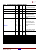
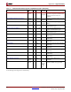
This section explains all of the timing parameters associated with the IBM PPC405
Processor Block. It is intended to be used in conjunction with Module 3 of the Virtex-II Pro
or Virtex-4 Data Sheet and the Timing Analyzer (TRCE) report from Xilinx software. For
specific timing parameter values and clocking considerations, refer to the appropriate data
sheet(s).
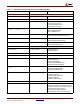
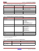
There are hundreds of signals entering and exiting the processor block. The model
presented in this section treats the processor block as a “black box.” Propagation delays
internal to the processor block and core logic are included in the processor block I/O
timing. Signals are characterized with setup and hold times for inputs and clock to valid
output times for outputs. Signals are grouped by the interface block from which they
originate: Processor Local Bus (PLB) , Device Control Register (DCR), External Interrupt
Controller (EIC), Reset (RST), Clock and Power Management (CPM), Debug (DBG),
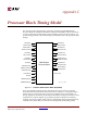
Figure C-1: PowerPC 405 Processor Block (Simplified)
CPM INPUT
CPM OUTPUT
RESET INPUT
RESET OUTPUT
PPC INPUT
PPC OUTPUT
PLB INPUT
PLB OUTPUT
OCM INPUT
OCM OUTPUT
DCR INPUTS
DCR OUTPUTS
JTAG INPUTS
JTAG OUTPUTS
TRACE INPUTS
TRACE OUTPUTS
DEBUG INPUTS
DEBUG OUTPUTS
EIC INPUT
CPMC405CLOCK
JTGC405TCK
PLBCLK
BRAMISCOMCLK
BRAMDSOCMCLK
IBM PPC405
Processor Block
UG012_C1_01_042304
FCM INPUTS*
*Virtex-4 Only
FCM OUTPUTS*
CPM FCMCLK*
CPM DCRCLK*