
User's Manual

PowerPC™ 405 Processor Block Reference Guide www.xilinx.com 93
UG018 (v2.0) August 20, 2004 1-800-255-7778
R
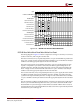
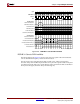
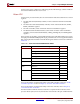
DSPLB Word Write/Word Read/Word Write/Line Read
The timing diagram in Figure 2-24 shows a sequence involving a word write, a word read,
another word write, and an eight-word line read.
The first word write (ww1) is requested by the DCU in cycle 2 and the BIU responds in the
same cycle. A single word is sent from the DCU to the BIU in cycle 2. The BIU uses the byte
enables to select the appropriate bytes from the write-data bus.
The first word read (rw2) is requested by the DCU in cycle 4. Even though the previous
request is completed in cycle 2, this is the earliest an address pipelined request can be
started by the DCU. The BIU responds in the same cycle the rw2 request is made by the
DCU. A single word is sent from the BIU to the DCU in cycle 5. The DCU uses the byte
enables to select the appropriate bytes from the write-data bus.
The second word write (ww3) is requested by the DCU in cycle 6. Again, this is the earliest
an address pipelined request can be started by the DCU. The BIU responds in the same
cycle the ww3 request is made by the DCU. A single word is sent from the DCU to the BIU
in cycle 6. The BIU uses the byte enables to select the appropriate bytes from the write-data
bus.
The line read (rl4) is address pipelined with the word write. The rl4 request is made by the
DCU in cycle 8 and the BIU responds in the same cycle. Data is sent from the BIU to the
DCU fill buffer in cycles 9 through 12. After all data associated with this line is read, it is
transferred by the DCU from the fill buffer to the data cache. This is represented by the fill4
transaction in cycles 13 through 15.
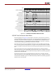
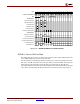
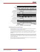
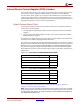
Figure 2-23: DSPLB Line Write/Line Read/Word Write
Cy cle
1 2 3 4 5 6 7 8 9 10 11 12 13 14 15 16 17 18 19 20
PLBCLK and CPMC40 5CLK
UG018_27_101701
PPC405 Outputs:
C405PLBDCUREQUEST
C405PLBDCURNW
C405PLBDCUABUS[0:31]
adr1 adr2
d3
adr3
flush1 fill2
C405PLBDCUBE[0:7]
C405PLBDCUWRDBUS[0:63]
C405PLBDCUSIZE2
DCU
rl2 ww3wl1
d1
01
d1
23
d1
45
d1
67
val
PLB/BIU Outputs:
PLBC405DCUADDRACK
PLBC405DCURDDBUS[0:63]
PLBC405DCURDWDADDR[1:3]
PLBC405DCURDDACK
PLBC405DCUWRDACK
PLBC405DCUBUSY
rl2 ww3wl1
wl1
01
wl1
23
wl1
45
wl1
67
ww3
d2
01
d2
23
d2
45
d2
67
0246
rl2
01
rl2
23
rl2
45
rl2
67