
Inc. Portable Generator User Manual

26 Xilinx Development System
Xilinx System Generator v2.1 Reference Guide
Addressable Shift Register
The Xilinx Addressable Shift Register block is a variable-length
shift register (or delay chain). This block differs from the Xilinx
Delay block in that the amount of latency experienced by data
frominput toblock output is variable and dependson theaddress
value.
Data presented to the block will traverse the entire delay chain.
The output of the block is not necessarily the output of the last register in the chain,
however. Instead, the output of the block is taken from the register pointed to by the
address presented on the addr port.
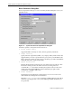
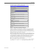
Block Interface
The block interface (inputs and outputs as seen on the Addressable Shift Register
icon) are as follows:
In Simulink, the addr port is given priority over the data (d) port, i.e. on each
successive cycle, the addressed data value is read from the register before the shift
operation occurs. This order is needed in the Simulink software model to guarantee
one clock cycle of latency between the data port and the first register of the delay
chain. (If theshift operation were tocome first,followedby theread,then there would
be no delay, and the hardware would be incorrect.)
Input signals:
d data input
addr address
en enable signal
Output signals:
q data output