
User's Manual

Virtex-5 FPGA ML561 User Guide www.xilinx.com 33
UG199 (v1.2) April 19, 2008
Power Regulation
R
The product specification at
http://www.displaytech.com.hk/pdf/graphic/64128e%20series-v10.PDF
provides more
information. Appendix C, “LCD Interface,” describes the LCD operation in detail.
Power Regulation
This section describes the devices that supply power to the Virtex-5 FPGA ML561
Development Board. For electrical requirements and power consumption, see Chapter 4,
“Electrical Requirements.”
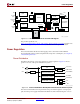
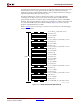
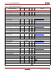
Power Distribution
The ML561 board uses +5V to drive numerous voltage regulators. Figure 3-9 shows a
general overview of the power distribution system.
The Virtex-5 FPGA ML561 Development Board is powered through the +5V input jack
(J28) from the power supply included in the ML561 Tool Kit. Alternatively, the +5V can
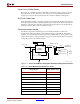
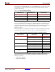
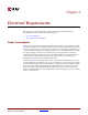
Figure 3-8: LCD Panel Connector for Possible LCD Support
HSTL
FPGA3
HSTL
V
TT
& V
REF
V
CCAUX
/
V
CCO
USB
DIP3
7SEG3
7SEG1
Config3
PROG
5V Input
Jack
5V Banana
Jacks
12V Input
Jack
SPY
SPY
OFF
OFF
ON
RESET
JTAG
UG199_c3_08_050106
System ACE
Controller
FPGA3 LEDs
JTAG Test Header
Test Header 3
A1
Serial Header
HSTL
12V -> 5V
RLDRAM II
QDRII
QDRII
RS232
Driver
RLDRAM II
3.3V
LCD Connector
Pwr Measure Header
LCD
Figure 3-9: Virtex-5 FPGA ML561 Development Board Power Distribution System
Board Power
3.3V
FPGA Power
V
CCINT
or V
CCAUX
/V
CCO
V
TT
V
TT
To FPGAs
To All FPGAs
To Memories
To Devices
V
REF
V
REF
MGT
Power
MGT Power
12V -> 5V
+12V
+5V
Slide
Switch
Slide
Switch
FPGA Power
SSTL18, HSTL, or SSTL2
Memory Power
SSTL18, HSTL, or SSTL2
UG199_c3_09_050106