
User's Manual

34 www.xilinx.com Virtex-5 FPGA ML561 User Guide
UG199 (v1.2) April 19, 2008
Chapter 3: Hardware Description
R
also be supplied from a bench supply using the two banana jacks: J25 (RED) for +5V and
J24 (BLACK) for GND.
The Rev-A assembly of the Virtex-5 FPGA ML561 Development Board does not support
the +12V input via jack J23 or via banana jacks J18 (RED) for +12V and J17 (BLACK) for
GND.
The memory and FPGAs use separate power supplies for SSTL18, HSTL, and SSTL2,
respectively. Thus the power being consumed can be easily measured for each using the
power measurement header provided on the ML561.
Voltage Regulators
The +5V voltage source is supplied as input to nine on-board regulator modules. Six of
those modules (TI PTH05010-WAZ) are used to generate the +1.0V, +2.5V, and +1.8V for
SSTL18 at FPGA #1 and FPGA #2, +1.8V for HSTL18 at FPGA #3, +2.6V for SSTL2 at
FPGA #1, and +3.3V voltages for the GTP power supplies, LEDs, etc. The remaining three
modules (TI PTH05000-ADJ) are used to generate +1.8V for SSTL18 at the memories, +1.8V
for HSTL at the memories, and +2.6V for SSTL2 at the memories.
An additional three bulk voltage regulators (Fairchild FN6555) are used to generate
termination (V
TT
) and reference (V
REF
) voltages each for the SSTL2, SSTL18, and HSTL
power levels. By design, these voltage levels are half of the input reference voltage being
supplied by the memory power supplies.
The TI PTH05010-WAZ and TI PTH05000-ADJ regulator modules require a fixed 5V input.
The output is adjustable over a range of 0.9V to 3.6V by changing the resistor tied between
pin 4 and GND. The difference between these two modules is that the PTH05010-WAZ
output voltage can be margined up to+ 5% of the nominal value by driving pin 10 to GND
(or digital Low), or margined down to -5% of the nominal value by driving pin 9 Low. The
PTH05010-WAZ also has a tracking feature that can be used to track another voltage
source.
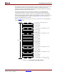
There are two ways to apply the digital controls to the margin input pins of the PTH05010:
either from FPGA #1 or manually with jumpers.
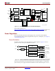
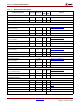
Figure 3-10: PTH05010 Voltage Regulator
PTH05010
Voltage Regulator
V
IN
GND
TRACK MRGN
UP
MRGN
DN
GND
C
IN
R
SET
470 μF
C
OUT
330 μF
(optional)
V
OUT
5V
+
+
1
2
3 5 4
6
7
8 9 10
Inhibit
Jumper
INHIBIT
V
O_ADJ
V
O_SENSE
VMARGIN_UP_xxxx_N
VMARGIN_DN_xxxx_N
TRACK
UG199_c3_10_050106