
Inc. Typewriter User Manual


MicroBlaze Processor Reference Guide www.xilinx.com 49
UG081 (v6.0) June 1, 2006 1-800-255-7778
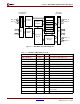
Local Memory Bus (LMB) Interface Description
R
Local Memory Bus (LMB) Interface Description
The LMB is a synchronous bus used primarily to access on-chip block RAM. It uses a
minimum numberof control signals anda simpleprotocol to ensurethat localblock RAM
areaccessedin a single clock cycle. LMBsignalsanddefinitionsareshown in the following
table. All LMB signals are active high.
LMB Signal Interface
Addr[0:31]
The address bus isan output from the core and indicatesthememory addressthat isbeing
accessed by the current transfer. It is valid only when AS is high. In multicycle accesses
(accesses requiring more than one clock cycle to complete), Addr[0:31] is valid only in the
first clock cycle of the transfer.
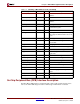
Byte_Enable[0:3]
Thebyte enablesignals areoutputs fromthe core and indicatewhich bytelanes ofthe data
bus contain valid data. Byte_Enable[0:3] is valid only when AS is high. In multicycle
accesses (accesses requiring more than one clock cycle to complete), Byte_Enable[0:3] is
valid only in the first clock cycle of the transfer. Valid values for Byte_Enable[0:3] are
shown in the following table:
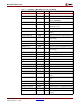
Table 2-2: LMB Bus Signals
Signal Data Interface
Instruction
Interface
Type Description
Addr[0:31] Data_Addr[0:31] Instr_Addr[0:31] O Address bus
Byte_Enable[0:3] Byte_Enable[0:3] not used O Byte enables
Data_Write[0:31] Data_Write[0:31] not used O Write data bus
AS D_AS I_AS O Address strobe
Read_Strobe Read_Strobe IFetch O Read in progress
Write_Strobe Write_Strobe not used O Write in progress
Data_Read[0:31] Data_Read[0:31] Instr[0:31] I Read data bus
Ready DReady IReady I Ready for next transfer
Clk Clk Clk I Bus clock
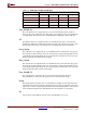
Table 2-3: Valid Values for Byte_Enable[0:3]
Byte Lanes Used
Byte_Enable[0:3] Data[0:7] Data[8:15] Data[16:23] Data[24:31]
0000
0001 x
0010 x
0100 x