
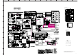
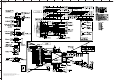
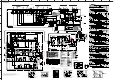
Service manual
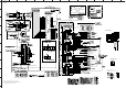
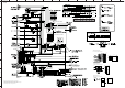


IC203
IC202
IC203
IC204IC205
IC206
IC201
A
1
2
3
4
5
6
7
8
9
10
BCDEFGH I JK
L MN
RX-V363/HTR-6130
74
★ All voltages are measured with a 10MΩ/V DC electronic voltmeter.
★ Components having special characteristics are marked s and must be replaced
with parts having specifications equal to those originally installed.
★ Schematic diagram is subject to change without notice.
DSP 2/6
3.4
3.4
3.4
00
03.4
0
0
01.6
0.9 0.3
0.9 1.6
2.1 0.3
2.1 1.6
00.3
1.6
0.3
3.4 3.4
1.6
0.3
3.5 1.7
0.2 0.3
0.2 1.7
2.0 0.3
1.8 1.7
1.9 0.3
1.9 3.4
1.9 0
1.9 3.5
3.3
0.2
3.4
3.4
3.4
3.4
3.4
3.4
0
3.4
1.6 3.4
1.6 3.4
1.6 3.4
1.6 3.4
1.6 3.4
1.7 3.4
1.7 3.4
1.7 0
0.3 0
0.3 0
0.3 0
0.3 0
0.3 0
0.3 0
0.3
0.3
0.2
0.2
0.9
1.3
0.2
2.1
0.2
2.1
2.0
3.4
1.8
3.4
1.9
3.4
1.9
3.3
1.9
1.9
1.8
3.3
3.4
0.2
0.3
3.4
0.3 3.4
0.3 3.4
0.3 3.3
0.3 3.4
0.3 3.3
0.3 1.7
0.3 3.3
0.3 3.4
0.3 3.4
1.7 3.4
1.7 0
1.7 3.3
1.6 3.4
1.6 0
1.6 0
1.6 0
1.6 0.5
03.4
0.3 3.4
0.3 1.4
0.3 1.4
0.3 0.8
0.3 0.8
0.3 5.0
0.3 3.4
0.3 0.2
0.3 0
03.4
0
3.4
4B
13
4A
12
4Y
11
3B
10
3A
9
3Y
8
1B
2
1Y
3
2A
4
2B
5
2Y
6
GND 7
IC203: SN74AHC02PWR
Quadruple 2-input positive-NOR gates
Vcc14
1A
1
IC204-206: SN74LV573APWR
Octal transparent D-type latches with 3-state outputs
1
2
3
4
5
6
7
8
9
10
20
19
18
17
16
15
14
13
12
11
OE
1D
2D
3D
4D
5D
6D
7D
8D
GND
V
CC
1Q
2Q
3Q
4Q
5Q
6Q
7Q
8Q
LE
OE
1
11
2
19
LE
1D
C1
1D
1Q
9
12
8D
C8
8D
8Q
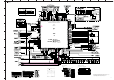
Bank Select
CLK
Row Decoder
I/O Control
Output Buffer
Sense AMP
Address Register
Data Input Register
Column Decoder
Latency & Burst Length
Programming Register
2M x 8 / 1M x16
2M x 8 / 1M x16
2M x 8 / 1M x16
2M x 8 / 1M x16
Col. Buffer
Row Buffer
Refresh Counter
ADD
LCKE
LRAS
CLK
LRAS
LCAS
Timing Register
LCBR LWE
DQi
LDQM
LWE
LWCBR
CKE CS
LCBR
WE L(U)DQM
LDQM
RAS CAS
1
VDD
VDD
VSS
N.C/RFU
VSS
VSS
VSSQ
VSSQ
VDDQ
VDDQ
DQ15
A4
A5
A6
A7
A8
A9
A11
CKE
CLK
N.C
DQ14
DQ13
DQ12
DQ11
DQ10
DQ9
DQ8
UDQM
V
DDQ
VDDQ
VSSQ
VSSQ
DQ0
DQ1
DQ2
DQ3
DQ4
DQ5
DQ6
DQ7
2
3
4
5
6
7
8
9
10
11
12
13
14
15
16
17
18
19
20
21
22
23
24
25
26
27
30
29
28
33
32
31
36
35
34
39
38
41
40
43
42
45
44
46
48
47
50
49
51
53
54
52
37
BA0
LDQM
VDD
WE
CAS
RAS
CS
BA1
A10/AP
A3
A0
A1
A2
IC202: K4S641632K-UC60000
64 M synchronous DRAM
to DSP 1/6
to DSP 1/6
to DSP 5/6
to DSP 4/6
to DSP 4/6
to DSP 3/6
to DSP 3/6, 4/6
to DSP 5/6
to DSP 3/6, 4/6, 6/6
to DSP 4/6
to DSP 5/6
to DSP 5/6
to DSP 1/6
to DSP 5/6
SDRAM
EXTENDED PORT
FLASH ROM
to DSP 4/6
to DSP 4/6
to DSP 5/6
to DSP 5/6