
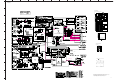
Service manual


CB512
CB501
CB502
CB516
CB504
IC501
IC501
IC501
IC501
IC505 IC505
IC505 IC505
A
1
2
3
4
5
6
7
8
9
10
BCDEFGH I JK
L MN
RX-V363/HTR-6130
77
★ All voltages are measured with a 10MΩ/V DC electronic voltmeter.
★ Components having special characteristics are marked s and must be replaced
with parts having specifications equal to those originally installed.
★ Schematic diagram is subject to change without notice.
DSP 5/6
3.4
3.4
3.4
3.4
3.4
3.4
0
3.4
3.4 3.4
4.9
3.4
3.4
4.9
3.4
3.4
0
0.8
0.8
0
1.3
1.3
0
3.4 3.4
3.4
A
B
C
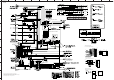
ANALOG L
FL
SW
SL
C
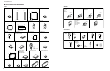
POINT A / EX3.3, B / Pin 8 of IC505, C / J504
Power cable ON Power cable OFF
EX3.3
IC505 8 pin
(/DRESET)
A
B
J504
(/RESET)
C
EX3.3
IC505 8 pin
(/DRESET)
A
B
J504
(/RESET)
C
Power cable ON
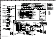
4B13
4A12
4Y11
3B10
3A9
3Y8
1B 2
1Y 3
2A 4
2B 5
2Y 6
GND 7
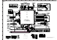
IC501: SN74AHCT08PWR
Quadruple 2-input positive-AND gates
Vcc141A 1
IC505: SN74LV08APWR
Quadruple 2-input positive-AND gate
4B13
4A12
4Y11
3B10
3A9
3Y8
1B 2
1Y 3
2A 4
2B 5
2Y 6
GND 7
Vcc141A 1
to DSP 1/6
to DSP 2/6
to DSP 3/6
to DSP 4/6
to DSP 4/6
to DSP 1/6
to DSP 2/6
to DSP 1/6-4/6
to DSP 2/6
to DSP 1/6, 2/6, 4/6
to DSP 1/6-4/6
to DSP 3/6
to DSP 3/6
to DSP 6/6
to DSP 6/6
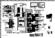
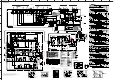
to MAIN (5)_CB161
Page 82
D10
to MAIN (1)_CB101
Page 81
A5
to MAIN (5)_CB164
Page 82
F4
to OPERATION (4)_CB182
(U, C models)
Page 80
K3
to OPERATION (2)_CB232
Page 80
A7