HOME THEATER SYSTEM AV-S70/NX-SW70 SERVICE MANUAL NX-SW70 is composed of SW-AVS70 and NX-AVS70s. SUBWOOFER (SW-AVS70) REAR SPEAKER (NX-AVS70) REAR SPEAKER (NX-AVS70) FRONT SPEAKER (AV-S70) IMPORTANT NOTICE This manual has been provided for the use of authorized YAMAHA Retailers and their service personnel. It has been assumed that basic service procedures inherent to the industry, and more specifically YAMAHA Products, are already known and understood by the users, and have therefore not been restated.
AV-S70/NX-SW70 ■ TO SERVICE PERSONNEL WALL OUTLET Critical Components Information. Components having special characteristics are marked Z and must be replaced with parts having specifications equal to those originally installed. EQUIPMENT UNDER TEST INSULATING TABLE ■ FRONT/REAR PANELS 170 (6–11/16") 100 (3–15/16") 10 (3/8") 30 (1–3/16") 241.2 (9–1/2") 110 (4–5/16") 41.
AV-S70/NX-SW70 ▼ SW-AVS70 399 (15–11/16") 335 (13–3/16") 24(15/16") 5.5 (3/16") AV-S70/NX-SW70 390.1 (15–3/8") 40 (1–3/4") 395.6 (15–9/16") 200.6 (7–7/8") ▼ NX-AVS70 111.5 (4–3/8") 20 (13/16") 140 (5–1/2") 100 (3–15/16") 1.
AV-S70/NX-SW70 ■ SPECIFICATIONS AV-S70 NX-SW70 ■ AMPLIFIER SECTION ■ AMPLIFIER SECTION Minimum RMS Output Power per Channel Front (1kHz, 10% THD, 6Ω) ........................... 30W + 30W Signal to Noise Ratio (IHF-A-Network) TV ............................................................................... 85dB Total Harmonic Distortion (1kHz) TV to Speaker Out, 12.5W/6Ω ................................ 0.08% Input Sensitivity/Impedance TV ..............................................................
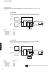
AV-S70/NX-SW70 ■ AV-S70 DISASSEMBLY PROCEDURES (Remove parts in the order as numbered.) 1. Removal of Grille Assembly. 2. Removal of Amplifier Unit a. Push up the Grille Assembly with a flat tip screwdriver or the like inserted from the bottom. (Fig. 1). a. Remove 4 wing screws (q) and then remove the Plate Legs (right and left). (Fig. 2) b. Keep pushing up the Grille Assembly gradually until it can be removed. b. Remove 4 screws (w). (Fig. 2) c.
AV-S70/NX-SW70 ■ TEST PROGRAM MODE (AV-S70) 1. Procedure for starting Test Program With the power turned off, press the POWER key while pressing the VOLUME key and the DSP key simultaneously. This initiates the Test Program function. When the Test Program is initiated, “01 DEST-Ex” appears on the FL display. 2. Procedure for selecting and executing Test Program Using the VOLUME + (UP) key and Volume - (DOWN) key, select the Test Program and then press the INPUT key to execute it. 3.
AV-S70/NX-SW70 Display Function The DSP DIAG (self-diagnosis) mode is initiated. (Refer to page 7 for the details.) 04 DSP Diag 05 Ver-A1.08 Microprocessor version / date display Example of microprocessor display 05 Ver-A1.08 Example of microprocessor date display 05 '99.10.15 What is displayed varies depending on the microprocessor software.
AV-S70/NX-SW70 ■ DSP DIAG MODE (Self-diagnosis) Use the remote controller supplied as an accessory to select the menu. 1. Procedure for starting DSP DIAG Referring to TEST PROGRAM MODE in the previous section, select/execute “04 DSP Diag”. When “04 DSP Diag” is executed, the current input name appears on the display followed by “Video” > “Sel.1to9 Key”. (The DSP indicator keeps flashing.) 2.
AV-S70/NX-SW70 Details of DIAG menu 1. Analog Thr. The input is fixed to use the analog (A/D) and has 2 sub-menu items. MAIN BYPSS The main L/R signal is output through the analog bypass without passing the DSP section. The main L/R signal passing through the DSP is output through C/LFE and RL/RR. CODEC.AD AC3Dav(YSS908) MAIN L ANALOG IN MAIN R CS4227 DECODER L/R DSP DIR2 L/R CODEC.
AV-S70/NX-SW70 2. DSP Through In the DIGITAL input mode, AC3/PCM AUDIO signal is automatically identified. There are 3 sub-menu items. YSS908-SRAM The main L/R signal is sent through AC3D2av into DSP. After passing through SRAM, the main L/R signal is output through L+R and C/LFE and RL/RR signals through (L+R)/2. CODEC.AD AC3Dav(YSS908) ANALOG IN CS4227 DECODER (L+R) DSP DIR2 (L+R) MAIN L MAIN R CODEC.
AV-S70/NX-SW70 DSP FULL BIT The main L/R is input through AC3D2av to DSP and then output through all channels. The head margin is eliminated and the digital data is output in digital full bit. The same applies as “YSS908” except that the digital data is output in full bit at D/A. AUX IN VOLUME : : – 20dBV, Both ch MAX : : : : : – 11dBV – 11dBV – 13dBV – 17dBV – 17dBV Full bit: The digital data is normally output with a head margin for each of C and RL/RR channels.
AV-S70/NX-SW70 4. Pro Logic The sub-menu items include selection of Pro-logic (The auto input balance is off.) and EFFECT OFF. CENTER LARGE When the analog, PCM audio or AC-3 2/0 mode is used, L, R, C, S signals are prologic decoded and output. When the AC-3 mode other than 2/0 is used, the pro logic function does not work and the signals are AC-3 reproduced. CODEC.AD AC3Dav(YSS908) ANALOG IN CS4227 DECODER DIR2 DOLBY DIGITAL or PRO LOGIC DSP L/R L/R C C S S CODEC.
AV-S70/NX-SW70 5. Speakers Set (for reference only) This menu is for checking during the production process and not for servicing. The input L/R signal is output through the specified channels according to the sub-menu. There are 7 sub-menu items. The signal output from the DSP section is normally in the EFFECT OFF state in the menus from 1 to 3. In the menus after that, the same signal as in the menu of 2. DSP THROUGH: YSS908 is output.
AV-S70/NX-SW70 6. Effect Off All effect functions are turned off. 7. Manual Test The test noise is output by the noise generator with a built-in DSP through the channels specified by the sub-menu. ALL MAIN L Noise is output through all channels. Noise is output through the MAIN L channel. CENTER Noise is output through the CENTER channel. MAIN R Noise is output through the MAIN R channel. REAR R Noise is output through the REAR R channel. REAR L Noise is output through the REAR L channel.
AV-S70/NX-SW70 ■ AV-S70 IC DATA 51 52 53 54 55 56 57 58 59 60 61 62 63 64 65 66 67 68 69 70 71 72 73 74 75 76 77 78 30 29 28 27 26 25 24 P24/FLD36 P25/FLD37 P26/FLD38 P27/FLD39 P30/FLD40 P31/FLD41 P32/FLD42 P33/FLD43 P34/FLD44 P35/FLD45 P36/FLD46 P37/FLD47 P40/FLD48 P41/FLD49 P42/FLD50 P43/FLD51 P44/TXD0/FLD52 P45/RXD0/FLD53 P46/CLK0/FLD54 P47/CTS0/RTS0/FLD55 P97/DA0/CLKOUT/DIMOUT P96/DA1/SCLK22 P95/SCLK21 P94/SOUT2 P93/SIN2 P92/SSTB2 P91/SBUSY2 P90/SRDY2 CNVSS P87/XCIN
AV-S70/NX-SW70 IC701 : M30218FCFP (16 bit µ-COM) AV-S70/NX-SW70 No.
AV-S70/NX-SW70 IC701 : M30218FCFP (16 bit µ-COM) ✽ No.
AV-S70/NX-SW70 FS1 32 KM0 DOUT 3 31 KM2 VFL 4 30 TSTN OPT 5 29 VSSa SYNC 6 28 CTLP MCC 7 27 (N.C.
AV-S70/NX-SW70 PVSS RAMD7 RAMD6 RAMD5 RAMD4 RAMD3 RAMD2 RAMD1 RAMD0 PVDD RAMA2 SCK SI SO /CS /CSB RAMA3 TEST /IC RAMA4 VSS RAMA5 RAMA6 /SDBCK0 SURENC KARAOKE MUTE CRC AC3DATA VDD IC4 : YSS908-F (P.C.B.
AV-S70/NX-SW70 IC4 : YSS908-F AC3Dav AV-S70/NX-SW70 No.
AV-S70/NX-SW70 IC4 : YSS908-F AC3Dav Name CRC MUTE KARAOKE SURENC /SDBCK0 RAMA6 RAMA5 VSS RAMA4 /IC TEST RAMA3 /CSB /CS SO SI SCK RAMA2 PVDD RAMD0 73 74 75 76 77 78 79 80 81 82 83 84 85 86 87 88 89 90 91 92 93 94 95 96 97 98 99 100 RAMD1 RAMD2 RAMD3 RAMD4 RAMD5 RAMD6 RAMD7 PVSS VDD2 SDWCK0 SDBCK0 SDIA0 SDIA1 RAMA1 RAMA0 RAMWEN RAMOEN VSS VDD IPORT7 IPORT6 IPORT5 IPORT4 IPORT3 IPORT2 IPORT1 IPORT0 VSS I/O O O O O O O O O I O I I O I I O I/O I/O I/O I/O I/O I/O I/O I/O I I I I O O O O I I I I I I I I F
AV-S70/NX-SW70 ■ AV-S70 BLOCK DIAGRAM (1/2) SIGNAL SENSOR L : 10 mV M : 5 mV H : 3mV M–SENSOR SELECTOR IC IC103 LC78212 CN105 4 IC107 1 5 R 13 2 9 10 IC10 M5220FP 7 IC102 Q101 Q102 RIN– 6 4 4 DIGITAL 6 1 1 2 IC9 7 RIN+ 1 LIN+ 12 L 21 13 R 22 4 3 25 26 M5220FP L : IC104 R : IC105 20 ML MR LFE 6 IC9 37 DATA 3 BC 7 WC 8 256FS 9 6 (25) 8 (23) 7 (24) 10 1 36 DSP–MASTER CLOCK/DATA 6 LOCKN PLL CONT Q1/Q2 6 7 9 (22) IC11 M5220FP 2 13 14 15 CN105 6 8 32 LFE 26
Q702 Q707 MUTE NIGHT DSP CONTROL SIGNAL SP-RY Q710 BASS BOOST SPRY NIGHT MUTE B–BST REM 27 23 19 17 8 3 94 93 2 1 21 16 63 100 89 97 +5V 32 34 65 14 30 33 15 FRX 13 VSS U701 VCC REMOTE SENSOR XL701 2 E PROM IC702 FCK AVSS E2CE AVCC FTX –25VEL –VP CLK 38 STB STB CE 28 CE DATA STANDBY LED KEY INPUT 96 98 IC701 M30218FCFP 29 31 ISEL–A VFL1 11 91 37 20 42 2 Page 38 VFL2 Q703 Q704 1 54 88 94 90 35 92 12 22 +5D Q701 Q708 P–ON SW–PRT SW
23 6 4 7 5 3 IC107 IC108 IC106 2 1 3 IC101 UPC4570 RELAY CONTROL 1 3 1 6 8 2 IC101 UPC4570 MUTE JK101 5 4 SW–PRT 4 Q109 Q110 Q111 Q112 D109 D108 Q102 Q101 IC103 UPC4570 2 8 9 T101 F101 IC109 STK408–040E 16 IC109 STK408–040E 12 R167 R168 6 RY103 Q104/Q105 OVER CURRENT DETECT 0.22Ω/3W METAL OXIDE FILM RESISTOR Q103/Q105 OVER CURRENT DETECT 0.
A B C D E F G H AV-S70/NX-SW70 ■ AV-S70 PRINTED CIRCUIT BOARD 1 DSP-FL ( A ) P. C. B. (Component side) DSP-FL ( A ) P. C. B. DIGITAL 1 1 CNVSS RESET VSS VCC CTSO CLKO RXDO TXDO CE L R CLKAC TXAC RXAC CEAC1 CEAC2 TCAC ERRA C LFE RL RR RIN LIN -25 +25 CDCOE SDT SCK CLD CCK CDO LOCKN ERR 4 DIGITAL 2 FROM : AMP (A) 3 FROM : DSP–FL (B) 2 (Foil side) FROM : DSP–FL (B) 5 ● Point q (Pin 13 of IC3) V : 2V/div, H : 0.1 µsec/div DC, 1 : 1 probe 0V 24 6 Semiconductor Location Ref. No.
A B C D E F G H AV-S70/NX-SW70 ■ AV-S70 PRINTED CIRCUIT BOARD 1 DSP–FL ( B ) P. C. B. (Component side) 3 +10 VPRT DGND +5D +5.6V –25V SW–PRT SW–RY SP–RY P–ON AMP–PRT B–BST MUTE NIGHT STB CLK DATA CE TruBass M–SENSOR ISEL–B ISEL–A PRE–OUT FROM : AMP (A) 2 Point w (Pin 13 of IC701) V : 2V/div, H : 0.
A B C D E F G H AV-S70/NX-SW70 ■ AV-S70 PRINTED CIRCUIT BOARD 1 AMP ( B ) P. C. B. AMP ( C ) P. C. B. (Component side) FROM : SPEAKER L 2 FROM : SPEAKER R AMP ( B ) P. C. B. (Component side) (Foil side) AMP ( C ) P. C. B.
A B C D E F G H AV-S70/NX-SW70 ■ AV-S70 PRINTED CIRCUIT BOARD 1 AMP ( A ) P. C. B. (Component side) AMP ( E ) P. C. B. AUX TV FROM : AMP (C) VIDEO TO : AMP (B) 2 THROU INPUT (Component side) MUTE +15 –15 SP–RY SW–PRT FROM : AMP (D) PRE–OUT TruBass AMP–PRT B–BST NIGHT 3 POWER 4 RE L RL R G RR SW G R L C LFE RL RR GND1 RIN LIN –25V +25V ● +10V DGND +5.
A B C D E F G H AV-S70/NX-SW70 ■ AV-S70 PRINTED CIRCUIT BOARD 1 AMP ( A ) P. C. B. AMP ( D ) P. C. B. (Component side) (Foil side) RE 2 TO : AMP (B) FROM : POWER CORD 3 YE TO : AMP (E) 4 RE RE RE TO : AMP (A) 5 ● Semiconductor Location Ref. No.
A B C D E F G H AV-S70/NX-SW70 ■ SW-AVS70 PRINTED CIRCUIT BOARD 1 AMP ( B ) P. C. B. (Component side) FROM : AMP (C) TO : SPEAKER WH 3 TO : AMP (A) TO : AMP (A) RE 2 RE (Component side) RE AMP ( A ) P. C. B. SYSTEM CONNECTOR REAR SPEAKER AMP ( C ) P. C. B. (Component side) RE FROM : AMP (B) RE 4 5 34 6 Semiconductor Location Ref. No. D101 D102 D103 D104 D105 D106 D107 D108 D109 D110 D111 D112 D113 Location C3 C4 C2 C3 C3 C3 B4 B4 A3 C3 C3 F4 F2 Ref. No.
A B C D E F G H I J K AV-S70/NX-SW70 ■ AV-S70 SCHEMATIC DIAGRAM (1/4) IC101 : TC4052BF Analog Multiplexers/Demultiplexers 1 REAR L P-37 J-4 22.5 0 0 –22.4 MAIN L 0 0 15 X3 11 Y0 1 Y1 5 Y2 2 Y3 4 7 SW 12 SW 0 14.5 0 DSP SW 0 SW SW 0x, 0y 1x, 1y 2x, 2y 3x, 3y NONE 0 0 0 0 0 0 0 0 4.8 0 0 0 –15.0 4.8 A 0 1 0 1 X 0 L1 1 30 R1 L2 2 29 R2 L3 3 28 R3 0 0 0 0 0 0 0 0 0 0 0 0 LCOM1 4 P-39 A-4 0 0 0 P-39 E-6 0 0 –7.
A B C D E F G H I J K L AV-S70/NX-SW70 ■ AV-S70 SCHEMATIC DIAGRAM (2/4) IC6 : CS4227-KP AD Converter/DA Converter LRCKAUX SCLKAUX NC DGND1 VD+ DGND2 SCLK LRCK SDOUT1 SDOUT2 SDIN1 1 P-38 F-6 44 43 42 41 40 39 38 37 36 35 34 33 SDIN2 0.1 0 2.9 0.3 0 0 0 0 4.7 AD1/CDIN AD0/CS SPI/I2C VD+ VA+ 7 40 19 DIR 4.6 0 4.
A B C D E F G H I J K AV-S70/NX-SW70 ■ AV-S70 SCHEMATIC DIAGRAM (3/4) ● V701 : 13-BT-169GNK (V4879700) 1 %9 q 2 –17.3 ● PIN CONNECTION P-39 J-7 CA404 –21.2 –21.2 –21.2 –21.2 –21.2 –21.2 –21.2 –22.5 –19.8 –17.1 –17.2 –19.8 –21.2 –19.9 –18.5 –22.5 –21.2 –18.5 ~ –18.5 –22.5 –21.2 ~ –22.5 ~ ~ ~ ~ –21.2 –18.5 ~ ~ –19.9 ~ ~ –17.2 ~ –17.3 –17.3 –17.3 –22.5 –21.1 –16.9 –21.1 –21.1 –21.2 –21.2 –21.2 –21.2 –21.2 –21.2 PATTERN AREA 17.4 –17.3 0 4.8 3 17.
A B C D E F G H I J K L AV-S70/NX-SW70 ■ AV-S70 SCHEMATIC DIAGRAM (4/4) –8.8 –15.0 820 0 0 120 0 2 8.7 –8.7 –8.7 0 0 0 0 0 8.7 0 0 8.7 8.7 8.7 –8.8 0 0 0 0 –8.8 8.7 –8.8 –8.8 4.8 MAIN L 0 0 –14.8 0 0 –3.1 30k 0 0 0 0 0 R533 MAIN L 0 14.7 0 0 0 –2.0 0 1.8 0 0 0 0 0 0 0 0 0 0 0 0 0 –2.1 1 0 28.7 –14.9 0 0 0 0 –29.0 0 14.6 4.8 0 14.6 3 –11.5 0 4.8 0 0 0 P-36 C-5 0 –11.5 0 0 0 P-36 H-3 4 0 –11.5 0 –29.0 0 28.
A B C D E F G H I J K AV-S70/NX-SW70 ■ SW-AVS70 SCHEMATIC DIAGRAM 1 27.5 11.9 0 2 –26.3 0 0 0 5.0 0 5.0 0 0 29.2 0 –29.3 –0.1 28.9 0 –27.5 0 0 0 28.8 0 –11.7 –11.5 0 29.2 REAR L 0 0 0 –11.5 28.8 0 SW 0 0 0 0 3 27.6 11.9 26.1 27.5 –0.1 0 11.7 0 0 0 0 0 0 0 0 0 –11.6 0 –1.5 0 0 0 0 5.0 0.2 0 12.0 –11.9 12.0 0 0 5.0 0 5 0 SW 0 0.2 Z 0 0 Z REAR L 11.9 Z 29.1 27.1 0 9.0 11.2 11.9 9.0 0 Z 29.2 12.
AV-S70/NX-SW70 PARTS LIST ■ ELECTRICAL PARTS ■ WARNING Components having special characteristics are marked Z and must be replaced with parts having specifications equal to those originally installed. ● Carbon resistors (1/6W or 1/4W) are not included in the ELECTRICAL PARTS List. For the parts No. of the carbon resistors, refer to last page.
AV-S70/NX-SW70 AV-S70 P.C.B. AMP * * * * * * * * * * * * * * * * * * * * * AV-S70/NX-SW70 * * * * * * * * * * * * * * * * * * * * * * * * * * * * Schm Ref. PART NO.
AV-S70/NX-SW70 AV-S70 P.C.B. AMP * * * * * * * * * * * * * * * * PART NO.
AV-S70/NX-SW70 AV-S70/NX-SW70 AV-S70 P.C.B. AMP & DSP-FL Schm Ref. PART NO.
AV-S70/NX-SW70 AV-S70 P.C.B. DSP-FL * * * * * * PART NO.
AV-S70/NX-SW70 AV-S70 P.C.B. DSP-FL * * * * * * AV-S70/NX-SW70 * * * * * Schm Ref. PART NO.
AV-S70/NX-SW70 CHIP RESISTORS Schm Ref.
AV-S70/NX-SW70 SW-AVS70 P.C.B. AMP * * * * * * * * * * * AV-S70/NX-SW70 * * * * * * * * * * * * * * * * * * * * * * * * * * * * * * * * * * * * * * * Schm Ref. PART NO.
AV-S70/NX-SW70 SW-AVS70 P.C.B. AMP Schm Ref.
1-11 1-11 7 50 1-12 2-6 2-8 2-19 2-19 2-7 3(E) 2-12 2-4 2-19 4(B) 1-1 1-12 2-19 2-19 2-19 1-10 1-6 2-21 2-19 3(D) 2-2-6 2-2-7 2-10 2-26 1-5 1-8 2-2-5 2-2-6 1-7 2-26 2-18 2-27 1-13 2-28 2-24 2-24 2-23 1-11 2-23 1-11 2-29 1-11 2-23 2-25 2-2-3 3(A) 2-24 2-24 4(A) 2-30 2-24 2-9 2-11 2-17 3(C) 2-5 2-24 200 200-1 2-25 2-25 C 1-2 2-13 2-22 2-3 1-4 2-19 5 1-9 2-16 1-8 3(B) 2-2-1 2-2-4 2-2-7 1-11 2-23 2-2-2 2 1-11 1-9 2-2-6 2-2-6 2-2-5 1-11
AV-S70/NX-SW70 ■ AV-S70 MECHANICAL PARTS * * * * * * * * * * * * * * * * * * * * Z * * * Z* * * * * * * * * * * PART NO.
AV-S70/NX-SW70 Ref. No. V5633900 AAX15160 AAX11350 AAX10940 AV-S70/NX-SW70 * 200 * 200-1 * * PART NO.
A B C D E AV-S70/NX-SW70 1 ■ SW-AVS70 EXPLODED VIEW 1-7 1-7 1-7 2-1 2-10 2-10 2-6 2-2 1-7 2-15 2-15 2 2-17 2-18 1-7 2-16 2-10 3(B) 2-3 2-7-1 2-7-3 2-7-2 2-12 2-7-7 2-13 2-7-4 3 2-11 1-7 1-3 1-7 2-7-5 2-7-6 2-18 2-9 2-9 2-17 3(A) 2-4 2-8 4 2-14 3(C) 2-5 1-1 1-2 1-6 5 1-4 1-6 4 1-4 1-8 207 6 202 1-5 206 204 203 205 7 53
AV-S70/NX-SW70 ■ SW-AVS70 MECHANICAL PARTS Ref. No. PART NO.
A B C D E AV-S70/NX-SW70 1 REMOTE CONTROL TRANSMITTER ■ SCHEMATIC DIAGRAM VDD VDD VDD VDD 38 17 C1 470µF C2 0.1µF 39 16 VDD R6 1kΩ VDD P21/TXD/S00 VSS C3 0.1µF 15 2 R2 1kΩ VSS P20/SCK0 27 6 28 5 14 VDD 8 SDA 7 NC 1 A0 2 A1 3 A2 X1 4.0MHz OPTION SCL C7 0.1µF X1 X2 IC2 VSS 4 C4 13 IC P47/KR7 VDD R7 470kΩ 18 K65 RESET C6 0.1µF VBAT 3 6 P46 P45 P44/KR4 7 P44 P43/KR3 8 P42/KR2 9 P43 P42 P41/KR1 10 P41 P40/KR0 11 NC 25 C5 0.
AV-S70/NX-SW70 Parts List for Carbon Resistors AV-S70/NX-SW70 Value 1.0 Ω 1.8 Ω 2.2 Ω 3.3 Ω 4.7 Ω 5.6 Ω 10 Ω 15 Ω 22 Ω 27 Ω 33 Ω 39 Ω 47 Ω 56 Ω 68 Ω 75 Ω 82 Ω 91 Ω 100 Ω 110 Ω 120 Ω 150 Ω 160 Ω 180 Ω 200 Ω 220 Ω 270 Ω 330 Ω 390 Ω 430 Ω 470 Ω 510 Ω 560 Ω 680 Ω 820 Ω 910 Ω 1.0 kΩ 1.2 kΩ 1.5 kΩ 1.8 kΩ 2.0 kΩ 2.2 kΩ 2.4 kΩ 2.7 kΩ 3.0 kΩ 3.3 kΩ 3.6 kΩ 3.9 kΩ 4.7 kΩ 5.1 kΩ 5.6 kΩ 6.8 kΩ 8.2 kΩ 9.1 kΩ 1/4W Type Part No. 1/6W Type Part No.