DRX-1 DRX-1 DVD RECORDER DRX-1 SERVICE MANUAL IMPORTANT NOTICE This manual has been provided for the use of authorized YAMAHA Retailers and their service personnel. It has been assumed that basic service procedures inherent to the industry, and more specifically YAMAHA Products, are already known and understood by the users, and have therefore not been restated.
DRX-1 DRX-1 ■ TO SERVICE PERSONNEL 1. Critical Components Information Components having special characteristics are marked s and must be replaced with parts having specifications equal to those originally installed. WALL OUTLET 2. Leakage Current Measurement (For 120V Models Only) When service has been completed, it is imperative to verify that all exposed conductive surfaces are properly insulated from supply circuits. ● Meter impedance should be equivalent to 1500 ohm shunted by 0.15µF.
DRX-1 DRX-1 Laser Diode Properties Type: Wave length: Output Power: (out of objective) Beam divergence: InGaAIP Semiconductor laser (DVD) AlGaAs Semiconductor laser (CD) 660 nm (DVD) 780 nm (VCD/CD) 20 mW (DVD writing) 0.8 mW (DVD reading) 0.3mW (CD reading) 82 degree (DVD) 54 degree (CD) VARO! : AVATTAESSA JA SUOJALUKITUS OHITETTAESSA OLET ALTTIINA NÄkymÄTTÖMÄLLE LASERSÄTEILYLLE. ÄLÄ KATSO SÄTEESEEN. VARNING! : OSYNLIG LASERSTRÅLNING NÄR DENNA DEL ÄR ÖPPNAD OCH SPÄRREN ÄR URKOPPLAD.
DRX-1 DRX-1 ■ PREVENTION OF ELECTRO STATIC DISCHARGE The laser diode in the DVDR mechanism may be damaged due to static electricity from clothes or the human body. Use caution to prevent electrostatic damage when servicing or handling the DVDR mechanism. 1. Grounding for electrostatic damage prevention Some devices, such as the DVD recorder, use an optical pickup (laser diode) that will be damaged by static electricity in the working environment.
DRX-1 DRX-1 ■ FRONT PANELS U model NATURAL SOUND DVD VIDEO RECORDER DRX-1 STANDBY STANDBY /ON REC DV S VIDEO VIDEO L AUDIO R TITLE SEARCH REC VOLUME AUTO/MAN MANUAL CHANNEL A model B model G model ■ REMOTE CONTROL MONTER A/CH 1 2 3 4 5 6 7 8 9 + CH – + – VOL SELECT CLEAR MUTE 0 TIMER RETURN OK ENTER TOP MENU SYSTEM MENU EDIT TITLE/CHAP SUBTITLE AUDIO ANGLE ZOOM A–B SHUFFLE SCAN REPEAT SKIP PLAY SEARCH/SLOW PAUSE STOP REC REC MODE DIMMER TV SHIFT DVD RECORDER
DRX-1 DRX-1 ■ REAR PANELS U model A, B, G models ■ SPECIFICATIONS DISC FORMATS SUPPORTED Disc type Playback DVD+RW • DVD+R • DVD-RW (Video format) • DVD-R • DVD-Video • SVCD • Video CD • Audio CD • CD-R • CD-RW • Recording • • — — — — — — — — RECORDABLE DISC FORMATS Medium DVD+RW: Phase-Change ReWritable DVD+R: dye-based Diameter 12 cm Capacity (single side) 4.7 Gbyte Recording time HQ 60’ 9.72 Mbit/s SP+ 150’ 4.06 Mbit/s EP 240’ 2.54 Mbit/s EP+ 360’ 1.
DRX-1 • DTS Multi-channel • MPEG1 2-channel Uncompressed digital (SPDIF) • PCM 2-channel 16, 20, 24 bit fs 48 kHz AUDIO PERFORMANCE DA Converter 24 bit AD Converter 16 bit DVD fs 96 kHz fs 48 kHz Video CD fs 44.1 kHz Audio CD fs 44.
DRX-1 DRX-1 VCR Plus+ and PlusCode are registered trademarks of Gemstar Development Corporation.The VCR Plus+ system is manufactured under license from Gemstar Development Corporation. Pats. 5,307,173; 5,335,079; 4,908,713; 4,751,578; and 4,706,121 Manufactured under license from Dolby Laboratories. “Dolby,” “Pro Logic” and the double-D symbol are trademarks of Dolby Laboratories. Confidential Unpublished Works. ©1992-1997 Dolby Laboratories, Inc. All rights reserved.
Display board 1001 ⇒ Remove 8 screws 31 → 38 (board → front) ⇒ demount the board IR/STBY Board 1001 ⇒ remove screws 41+42 (board → front) ⇒ demount the board for screws 21, 34 and 35 for screws 32 for screws 22, 31 and 33 2.7 mm 2.2 mm 1.7 mm T10 T8 T6 mounting ↑ ↓ demounting Digital board 1001 ⇒ Remove the connections ⇒ Remove 4 scrws 207 → 210 (Digital board → frame 181) ⇒ demount the board.
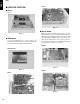
DRX-1 DRX-1 ■ SERVICE POSITION DVIO 2 ● Front Front Photo 4 ● Digital board Photo 1 ● DVIO board To put the DVIO board in a service position, an extender board must be used. This extender board can be ordered with codenumber 3104 128 07770. After demounting of DVIO board, the top side of the digital board is in reach. To reach the bottom side of the digital board, the DVDR module must be demounted together with the digital board.
DRX-1 DRX-1 ● Analog board 1. 2. 3. 4. To put the analog board in service position, demount the assembly of analog board and backplate as follows: Remove 3 screws from the backplate to the frame Remove the screw from the backplate to the mains inlet of the power supply Remove the screw of the analog board to the frame Release the snaps of the 4 spacers of the analog board to the frame. Turn the assembly of the backplate and the analog board against the loader.
DRX-1 DRX-1 ■ DIAGNOSTIC SOFTWARE Due to the complexity of the DVD recorder, the time to find a defect in the recorder can become long. To reduce this time, the recorder has been equipped with Diagnostic and Service software (DS). The DS offers functionality to diagnose the DVDR hardware and tests the following: • Interconnections between components • Accessibility of components • Functionality of the audio and video paths This functionality can be accessed via several interfaces: 1.
DRX-1 DRX-1 3 706 AnalogueTuner checks whether the tuner on the analogue board is accessible 2 901 LoopAudioUserDealer This nucleus tests the components on the audio signal path The host decoder - The analogue board - The audio encoder - The VSM On the analogue board the audio is internally looped back to the digital board 1 906 LoopVideoUserDealer Nucleus for testing the components on the video signal system path: - The VIP - The video encoder - The VSM - The host decoder - The analogue board
DRX-1 DRX-1 14 STEP DESCRIPTION NUCLEUS 5 The local display shows FPLED. Press PLAY to start the test. Press PLAY to confirm that the led is lit. Press RECORD to indicate that the led is not lit. Press STOP to skip this nucleus. 504 6 The local display shows FPFLAP OPEN. Press PLAY to start the test. Press PLAY to confirm that the flap has opened. Press RECORD to indicate that the flap did not open. Press STOP to skip this nucleus. 522 7 The local display shows FPKEYBOARD.
DRX-1 NUCLEUS 22 The local display shows BEWRITE READ. Press PLAY to start the test. Press STOP to skip this nucleus. 617 23 The local display shows BETRAY OPEN. Press PLAY to start the test. Press STOP to skip this nucleus. 616 24 The local display shows BETRAY CLOSE. Press PLAY to start the test. Press STOP to skip this nucleus. 615 25 The local display shows READ ERRORLOG. Press PLAY to start the test. Press STOP to skip this nucleus.
Fig.
DRX-1 DRX-1 FRONTPANEL TEST DIGITAL BOARD & ANALOG BOARD TEST BASIC ENGINE TEST press to execute press < STOP > to skip press to execute press to skip press to execute press < STOP > to skip press to execute press to skip INSERT DVD +RW DISC TO EXECUTE WRITE / READ TEST press to execute press < STOP > to skip press to execute press to skip press to execute press < STOP > to skip press to execute press to skip
DRX-1 DRX-1 2.4 Trade Mode IF TRADE MODE OFF IF TRADE MODE ON UNPLUG THE RECORDER UNPLUG THE RECORDER PRESS 2 KEYS SIMULTANEOUSLY 3.2 Error Handling Each nucleus returns an error code.
DRX-1 Host Decoder [01] [xxyy] Nuclei Number 100 Checksum Flash 101 Flash Write Access 1 102 Flash Write Access 2 103 Flash Write Read 104 SdRam Write Read 105 SdRam Write Read Fast 106 Dram Write Read 107 Dram Write Read Fast 108 Hardware Version 109 Mute On 110 Mute Off 115 Pink Noise On 116 Pink Noise Off 117 Sine On 118 Sine Burst 1kHz 119 Sine Burst 12kHz 120 Colour-bar On 121 Colour-bar Off 122 NvramWrR 123 NvramI2c 130 Boot Version 131 Application Version
DRX-1 DRX-1 Basic Engine [06] [xxyy] [xxyy] Number Nuclei Number 718 Download Version 600 S2B Pass 720 Bargraph Level Adjustment 601 S2B Echo 721 Clock correction 602 Version 722 Clock reference 603 Reset 723 Re-virginise Recorder 604 Focus On 724 Flash Checksum 605 Focus Off 725 Tuner frequency selection 606 Disc Motor On 727 Set virgin bit 607 Disc Motor Off 728 Clear Virgin Bit 608 Radial On 729 Write / read I2C message to / from analogue board 609 Radial Of
DRX-1 [xxyy] Nuclei Number 1400 Clock 11.289 MHz 1401 Clock 12.288 MHz 1412 Progressive Scan I2C 1413 Progressive Scan test image on 1414 Progressive Scan test image off 1415 Progressive Scan Route Enable 1416 Progressive Scan Route Disable Scripts [00] [xxyy] Nuclei Number 1 Us erDealer Script 2 Pl ayer Script 3.
DRX-1 DRX-1 Sine Generate Menu 1.Sine On 2.Sine Burst 1kHz 3.Sine Burst 12kHz VSM Menu 1.Register Access 2.SDRAM Access 3.VSM SDRAM Write/Read 4.Interrupt Lines 5.VSM Interconnection 6.UART AVENC Menu 1.Empress 2.Video Input Processors -> -> Empress Menu 1.Version number Video Input Processors Menu 1.SAA7118 I2C Access NVRAM Menu 1.Read Error Log 2.Reset Error Log 3.Read DVIO Unique ID Analogue Board Menu 1.Echo 2.Obsolete 3.Route Video Input back to Digital board 4.
DRX-1 DRX-1 Basic Engine Radial Menu 1.Radial On 2.Radial Off 3.Radial Initialisation 4.Radial ATLS Calibration Script Menu 1.User/Dealer Script 2.Player Script 4. Nuclei Error Codes In the following table the error codes will be described. Basic Engine Sledge Menu 1.Sledge test 2.Sledge test slow Basic Engine Tray Menu 1.Tray In 2.Tray Out DVIO Menu 1.Check Presence 2.Reset 3.Access 4.Error Codes 5.Module Identifiers 6.Led -> DVIO Led Menu 1.Led On 2.Led Off Progressive Scan Board Menu 1.
DRX-1 DRX-1 24 Error Nr Error String Error Nr Error String 11500 “” 13700 “” 11501 “Init of I2C failed” 13701 “Turning off MacroVision failed” 11502 “The selection of the clock source failed” 20000 “” 11504 “The demute of the audio failed” 20001 “I2C bus busy before start” 11600 “” 20002 “Video Encoder access time-out” 11601 “Init of I2C failed” 20003 “No acknowledge from Video Encoder” 11602 “The mute of the audio failed” 20004 11700 “” “No data send/received to or from
DRX-1 Nr Error String Error Nr Error String “” 20902 “I2C bus busy before start” 20501 “Error audio encoder SRAM WRR cannot initialise I2C” 20903 “EMPRESS access time-out” 20904 “No acknowledge from the EMPRESS” “Error audio encoder SRAM WRR cannot reset DSP through I2C” 20905 “No data send to the EMPRESS” “Error audio encoder WRR cannot download boot” 20906 “No data received from the EMPRESS” 30000 “” 30001 “VSM SDRAM Bank1 Memory databus test goes wrong.
DRX-1 DRX-1 Error Nr Error String Error Nr Error String 30304 “Interrupt B wasn’t raised.” 50103 30305 “Interrupts A and B were raised.” “The frontpanel could not be accessed by the ana-logue board.” 30400 “” 50200 “” 30401 “VSM SDRAM Bank1 Memory databus test goes wrong.” 50204 “Execution of the command on the analogue board failed.” 30402 “VSM SDRAM Bank1 Memory addressbus test goes wrong.” 50205 “The frontpanel could not be accessed by the ana-logue board.
DRX-1 Nr Error String Error Nr Error String “The frontpanel did not show a starburst.” 51701 50704 “The user skipped the FP-starburst test.” “Execution of the command on the analogue board failed.” 50705 “The user returned an unknown confirmation: con-firmation” 51702 “The frontpanel could not be accessed by the ana-logue board.” 50800 “” 51703 “The VU grid did not display properly.” 50801 “Execution of the command on the analogue board failed.” 51704 “The user skipped the VU gridtest.
DRX-1 DRX-1 Error Nr Error String Error Nr Error String 60106 “Wrong echo pattern received” 61502 “Parity error from Basic Engine to Serial” 60200 “Version: nr1.nr2.
DRX-1 Nr Error String Error Nr Error String 61905 “Unexpected response from Basic Engine” 62900 “” 62000 “” 62901 62001 “Self-Test : errorstring1 Laser-Test : errorstring2 SpindleM-Test: errorstring3 Sledg-eM-Test : errorstring4 Focus-Test : errorstring5” “Basic Engine returned error number 0xerrornumber” 62100 “The forward sense level is 0xlevel” 62101 “Basic Engine returned error number 0xerrornumber” 62902 “Parity error from Basic Engine to Serial” 62903 “Communication time-out error
DRX-1 DRX-1 30 Error Nr Error String Error Nr Error String 63901 “Basic Engine returned error number 0xerrornumber” 64201 “BE i2c initialisation failed” 64202 63902 “Parity error from Basic Engine to Serial” “This nucleus cannot be executed because the Self-Test failed” 63903 “Communication time-out error” 70000 “Echo test OK” 63904 “Unexpected response from Basic Engine” 70001 “Echo test returned wrong string.
DRX-1 DRX-1 Error Nr Error String Error Nr Error String 71301 “Routing the audio on the Analogue Board fails.” 73002 “Communication with Analogue Board fails” 73100 71302 “Invalid input.” “0xslashversion”” where slashversion is the slash version read from the analogue board” 71303 “Communication with Analogue Board fails” 73101 “Error while reading out slash version.” 71500 “” 73102 “I2C Write error.” 71501 “Invalid slash version, default slash version is set.
DRX-1 DRX-1 32 Error Nr Error String Error Nr Error String 80300 “The accessibility of the DVIO module is OK.” 80412 80301 “The DVIO board is not present in this DVDR.” “We tried to receive a reply for DVIO_MAX_RETRIES_REPLY times !!” 80302 “Could not initialise I2C.” 80413 80303 “Unable to reset the DVIO module.” “We tried to receive an Ack for DVIO_MAX_RETRIES_ACK times!!” 80304 “Unable to receive the reset indication from the DVIO module.
DRX-1 Nr Error String Error Nr Error String “The DVIO module could not be reset.” 80713 80604 “Unable to receive the reset indication from the DVIO module.” “We tried to receive an Acknowledge for DVIO_MAX_RETRIES_ACK times!” 80714 80605 “Unable to send the configuration to the DVIO module.” “VSM UART error timeout transmitting command” 80715 “VSM UART error timeout receiving reply” 80606 “Unable to download the chip ID to the DVIO mod-ule.
DRX-1 DRX-1 Error Nr Error String Error Nr Error String 90221 “The video encoder did not receive data from the VIP.” 90420 “The video encoder did not return the Group Of Picture count.” 90223 “Initialisation of VIP and EMPRESS failed” 90421 90224 “The video encoder did not return the current sta-tus.” “The video encoder did not receive data from the VIP.” 90422 90225 “The video encoder timed out in BUSY mode. (no VIP input)” “Execution of the command on the analogue board failed.
DRX-1 Nr Error String Error Nr Error String 90617 “VSM and Hostdec memory do not match (com-pared after transfer)” 90812 “Error cannot initialise host decoder audio in” 90813 90618 “Decoding of the video data in the hostdecoder memory failed” “Error loop audio user/dealer cannot start audio en-coder” 90619 “The data in the hostdecoder is not equal to a col-ourbar” 90620 “The video encoder did not return the Group Of Picture count.” 90621 “The video encoder did not receive data from the VIP.
DRX-1 DRX-1 Error Nr Error String Error 90920 “Error: audio data in host memory and VSM mem-ory differ” 141301 “Progressive Scan Route Enable failed” 90921 “Error: audio data in host memory contains wrong frequency: frequency Hz” 141400 “” 90922 “Error: audio data in host memory contains silence!” 141402 “Turning off test image in Hostdecoder failed” 90923 “There is no correct audio frame in the buffer” 90924 “The audio frame has an illegal version bit” 90925 “The audio frame has an illeg
DRX-1 DRX-1 5.2 Nucleus 901: Audio User Dealer Loop A PCM audio sine of 12kHz is generated in the Host Decoder for a while and sent to the analogue board. The signal coming from the analogue board is encoded again and sent to the memory of the host decoder for comparison.
DRX-1 DRX-1 5.4 Nucleus 903: Digital Video VBI Loop Nucleus for testing the components on the video VBI signal path: • The VIP • The VSM • The Host Decoder This is done by using the internal test signal source (digital board only) Remark: this test is only successful if nucleus 121 is carried out first. 5.
DRX-1 DRX-1 5.6 Nucleus 905: System Video VBI Loop This nucleus tests the components on the video signal path: • The VIP • The VSM • The Host Decoder The video CVBS signal is routed to the output of the analogue board where it will be looped back by means of an external cable. Remark: this test is only successful if nucleus 121 is carried out first. 5.
DRX-1 DRX-1 5.8 Nucleus 907: Video VBI User Dealer Loop This nucleus tests the components on the video VBI signal path: • The VIP • The VSM • The Host Decoder The signal is routed back internally on the analogue board Remark: this test is only successful if nucleus 121 is carried out first. 5.
DRX-1 DRX-1 5.10 Nucleus 909: System Audio Loop CINCH (Nafta) Nucleus for testing the components on the audio signal path: • The hostdecoder • The analogue board • The audio encoder • The VSM On the analogue board the audio is passed to the CINCH connector, where a CINCH cable needs to be used to loop back the audio signal to the digital board.
DRX-1 DRX-1 ■ FAULTFINDING TREES 1. General-1 PLAYBACK MODE Plug Recorder to the mains. No disc loaded Standby LED changes from green to red. Display shows time NOK Check PSU(see chapter 2) Check Analog PCB(see chapter 4) Check Display PCB(see chapter 5) OK Press "STOP" button Standby LED changes from Red to Green. Display shows successively "READING" "NO DISC" OK NOK Check Trade Mode(see DIAGNOSTIC SOFTWAE chapter 2.
DRX-1 DRX-1 1. General-2 RECORD MODE Insert DVDR Disc Display shows: - Disc content - Source - DVD+RW - Disc Bar NOK - Check Basic Engine(see chapter 3) OK Press NEXT button to select empty title Press "RECORD" button Recording starts NOK OK - Check Analog PCB(see chapter 4) - Check Digital PCB(see chapter 3) - Check Basic Engine(see chapter 3) - Check DVDR Disc Press "STOP" button Menu update Check recorded title NOK - Check Basic Engine(see chapter 3) - Check DVDR Disc OK Recording OK Fig.
DRX-1 DRX-1 2. Power Supply Remove all the connectors from the PSU Check DC voltages on connector 0205: +12Vstby, +5V2stby, -5Nstby, -Vgnstby, +33Vstby None of the voltages are present +12Vstby and +5V2stby are OK. All voltages are present.
DRX-1 DRX-1 3. Digital Board-1 START UP DSW NOT OK OK Check Power Supplies on con.
DRX-1 DRX-1 3.
DRX-1 DRX-1 3.
DRX-1 DRX-1 3.
DRX-1 DRX-1 3. Digital Board-5 DSW VSM TESTS Start Diagnostic Software and select Command mode VSM Interconnection Test Command: 304 NOK - Check IC 7100 OK SDRAM Access Test Command: 301 NOK - Check IC 7101 OK SDRAM Write/Read Test Command: 302 NOK - Check IC 7100 - Check IC 7101 NOK - Check IC 7100 - Check IC 7101 OK VSM Interrupt Test Command: 303 OK VSM Connection to analog board Test Command: 305 NOK - Check IC 7100 - Check connection to analog board OK VSM PART OK Fig.
DRX-1 DRX-1 3. Digital Board-6 DSW AUDIO PART CHECK Start Diagnostic Software and select Command mode Audio Clock Test Command: 1400 Measure ACC_ACLK_PLL on I902 (11.289MHz) NOK - Check IC 7900 - Check IC 7906 - Check IC 7100 OK Audio Clock Test Command: 1401 Measure ACC_ACLK_PLL on I902 (12.288MHz) NOK - Check IC 7900 - Check IC 7906 - Check IC 7100 OK Host Pink Noise ON Command: 115 Check AD_BCLK(3.072MHz) on pin14 of con.1602 Check AD_WCLK(48KHz) on pin12 of con.1602 Check AD_ACLK(12.
DRX-1 DRX-1 3. Digital Board-7 DSW VIDEO PART CHECK Start Diagnostic Software and select Command mode Gateway Test to Analog Board Command: 700 NOK - Check Analog Board - Check IC 7100 OK Color Bar ON Test Command: 120 OK Check Red Video Out on pin 5 of con.1601 Check Green Video Out on pin 3 of con.1601 Check Blue Video Out on pin 1 of con.1601 Check CVBS Video Out on pin 11 of con.1601 Check Y-Video Out on pin 9 of con.1601 Check C-Video Out on pin 7 of con.
DRX-1 DRX-1 3.
DRX-1 DRX-1 3. Digital Board-9 DSW BASIC ENGINE TESTS Start Diagnostic Software and select Command mode Basic Engine S2B Echo Test Command: 601 NOK - Check IC 7202 - Check Basic Engine OK Basic Engine Tray Open Test Command: 616 NOK - Check Basic Engine OK Insert a DVDRW video disc OK Basic Engine Tray Close Test Command: 615 NOK - Check Basic Engine OK Basic Engine S2B Write Read Test Command: 617 NOK - Check Basic Engine - Check IC 7100 OK BASIC ENGINE PART OK Fig.
DRX-1 DRX-1 3. Digital Board-10 Waveforms Digital Board Sysclk_5505 Sysclk_VSM 2V / div DC 20ns / div 2V / div DC acc_aclk_pll 27M_clk_PS 2V / div DC 20ns / div 2V / div DC 10ns / div 2V / div DC VIP_ICLK 2V / div DC 10ms / div VSM_M_CLK 20ns / div 2V / div DC Fig.
DRX-1 DRX-1 3.
DRX-1 DRX-1 3. Digital Board-12 Waveforms Digital Board 500mV / div AC 10us / div 10us / div 10ms / div Y-signal 500mV / div AC 2V / div DC 2V / div DC 10us / div 500mV / div AC 20us /div Fig.
Measurement Point Overview for A, B, G models -2 4. Analog Board-1 DRX-1 Measurement Point Overview for A, B, G models -1 DRX-1 Fig.
Measurement Point Overview for A, B, G models -3 Measurement Point Overview for U model -1 DRX-1 DRX-1 4. Analog Board-2 Fig.
Measurement Point Overview for U model -3 4. Analog Board-3 DRX-1 Measurement Point Overview for U model -2 DRX-1 Fig.
DRX-1 DRX-1 4.
DRX-1 DRX-1 4.
DRX-1 DRX-1 4. Analog Board-6 Routing Audio and Video Route Video Nucleus Number: 712 Description This nucleus routes the video signals on the analogue board to the destination determined by the input parameters. The paths that are available for video routing and their description(Europe version) The paths that are available for video routing and their description (Nafta region) routed to the digital board.
DRX-1 DRX-1 4. Analog Board-7 Route Audio Nucleus Number: 713 Description This nucleus routes the audio on the analogue board to the destination determined by the input parameters. The paths that are available for audio routing and their description (Europe version) PATH ID DESCRIPTION 00 01 Input signal is VIDEO(CVBS) from digital board and will be re-routed back to the digital board. Input signal is from FRONT AUDIO IN and will be routed to the digital board.
DRX-1 DRX-1 5. Display Board TROUBLESHOOTING DISPLAY BOARD Check supply voltage NO DISC POWER ON Connector1916-2 Connector1916-3 Connector1916-11 Connector1916-12 12STBY VGNSTB 5STBY 5M +12V -32V +5V +5.2V Check filament voltage NO DISPLAY? Testpoint F105 12STBYSI AC voltage is created via oscillator circuit (7152-7153). Check heater voltage on testpoints F102 and F101 +12V 3.2VAC, -24,4VDC, 42 kHz.
DRX-1 DRX-1 6.
DRX-1 DRX-1 6. DVIO Board-2 RESET & CLOCK CHECK DVIO USE DVIO BOARD CIRCUIT DIAGRAMS 2, 3, 4 AND 5 AND DVIO TOP VIEW TEST POINTS Power On and exit stand-by mode Enable DVIO board: - press channel up or down untill the display shows CAM3 - press tuner key in order to switch to the DV-source The red LED above the DV-input will light up.
DRX-1 DRX-1 6.
DRX-1 DRX-1 6. DVIO Board-4 Waveforms DVIO uP_clock 2V / div DC Clockaudtmp 100ns / div 2V / div DC Clock 27MHz 2V / div DC Clock 27M_DV 20ns / div 2V / div DC Clock 27M_CON 2V / div DC 20ns / div Fig.
DRX-1 1. Alignment Instructions Analogue Board Alignments Analog PCB Eur ADJUSTMENT INSTRUCTIONS ANALOGUE BOARD Test equipment: 1. Dual-trace oscilloscope Voltage range : 0.001 ~ 50 V/div Frequency : DC ~ 50 MHz Probe : 10:1, 1:1 2. DVM (Digital voltmeter) 3. Frequency counter 4. Sinus generator Sinus : 0 ~ 50 MHz 5.
DRX-1 DRX-1 2.1 Bargraph 0db Alignment For an exact functionality of the bar graph in the display, a correction factor for the left and the right channel is stored in the NVM. Procedure: • Put the set in DSW command mode • route Audio path from Audio front connectors to digital with the following command: DD:> 713 01 • apply a sine wave of 1 kHz, 1.
DRX-1 DRX-1 3.4 Procedure B 1. Note the serial number of the set example: AH050136130156 – AH = production centre Hasselt. According to UAW500: A=1 and H=8 – 05 = change code (this is not used for this calculation) – 01 = YEAR – 36 = Production WEEK – 130156 = Lot and SERIAL number 2. Calculate the unique number: this number always exists out of 10 hexadecimal numbers. 3.
DRX-1 DRX-1 ■ CIRCUIT DESCRIPTION 1. Multi-Mode SOPS 50PS203 1.1. Why Multi-Mode SOPS? Using ordinary SOPS results in a decrease of the efficiency at low output loads due to the increase of the switching frequency. The Multi-Mode SOPS will reduce the switching frequency at low loads but still preserves valley switching. 1.2.
DRX-1 Overvoltage Protection Circuit This circuit consists of R3149, D6144, 6143, R3144, C2142 and T7142. When the regulation circuit is interrupted due to an error in the control loop, the regulated output voltage will increase (overvoltage). This overvoltage is sensed on the primary winding 7-8. When an overvoltage is detected, the circuit will start up the thyristor circuit T7141-7143. The power supply will come in a hiccup mode as long as the error in the control loop is present.
DRX-1 DRX-1 2. Display Board 2.1 Operation Unit DC (DC Part) The core element of the operation unit DC is the microcontroller TMP88CU77ZF [7156]. The TMP88CU77ZF is an 8 bit microcontroller fitted with 96kB ROM and 3kB RAM and is responsible for following functions: • Integrated VFD driver • Timer • Evaluation of the keyboard matrix • Decoding the remote control commands from the infrared receiver pos.
DRX-1 3.1 Microprocessor TMP93C071F The microcontroller „AIO“ TMP93C071F is a 16bit microcontroller with internal ROM and 8kB RAM. It includes the following functions: • A/D converters • composite sync input • I2C bus interface Following connection to the mains, a positive pulse on the reset input on the P is generated by the reset-IC TL7705 (Pos.7900). The system clock is generated with the 20MHz quartz (Pos. 1994). 3.
DRX-1 DRX-1 determine the antenna signal strength after a buffer [7705] with the signal AGC_MUTE. In the opposite direction this line may be used to mute the demodulator to avoid cross talk in all cases, where the tuner signal is not needed. In this case a „high“ signal is sent via AGC_MUTE and the conducting diode [6703] to pin4. The video trap [1703] reduces adjacent channel video and sound carrier remainders in the video for BG standards.
DRX-1 Pin-16 (Fast Blank): Only the status/level of Scart-2/Pin16 must be detected; this is realised by using PortC3/AIN14 (Pin25) of the CC-C as an Analogue-input. • ADC-value lower or equal 24h ( Pin16 low (no RGBsignals) • ADC-value greater 24h ( Pin16 high (RGB present on Scart-2) To avoid misdetection a “software-integration” (result is first valid if it was 3-times the same) must be implemented, determination has to be done approx. every 47msec (no multiple of V-sync).
Fig.
AL 4 6 I2S AFCRI AFCLI AR AL Rear Cinch 1958 out FROM DIGITAL BOARD 1900 1953 Front Cinch in FRONT END FROM FRONT A/V BOARD 3 DAC UDA1328 12 SIF1 DVAR DVAL ARCLI ARCLI 1705 7703 DV-Audio in 1960 FROM AR DVIO BOARD 8 5 1958 Rear Cinch in 41 40 38 15 7 7002 11 MC33078 12 2 MSP3415 8 19 37 7001 20 ALDAC ARDAC 30 AFER 6 3 2 4 1 I2C 1 4 GIN_ENC 44 CIN_VCR 48 CIN_ENC 40 RCIN_AUX 28 RCIN_ENC 42 CIN_TV 54 34 SDA 22 SCL 21 RIN_AUX 37 RIN_VCR 47 RIN_TV
DRX-1 DRX-1 4. Analog Board Nafta version 4.1 Microprocessor TMP93C071F The microcontroller „AIO“ TMP93C071F is a 16bit microcontroller with internal ROM and 8kB RAM. It includes the following functions: • A/D converters • composite sync input • I2C bus interface The following connection to the mains, a positive pulse on the reset input on the P is generated by the reset-IC TL7705 (Pos.7900). The system clock is generated with the 20MHz quartz (Pos. 1994). 4.
DRX-1 CVBS Signals: There are two CVBS input connection possibilities: Front chinch (E5) and Rear Chinch In (E3). Both CVBS sources are connected direct to the STV 6410 and routed to Rear Out 1 and Rear Out 2 via the 75-Ohm driver BA 7623. Both CVBS output sockets are connected to BA 7623 in parallel. Independent of the input signal quality (CVBS, S-Video or Y/UV) the digital board supplies also S-Video and Y/UV signals to the corresponding sockets.
DRX-1 DRX-1 Detailed Description UDA 1328: The UDA1328 is a 6 channel DAC employing bitstream conversion techniques, which can be used either in L3 microcontroller mode or in static pin mode. The UDA 1328 supports the I2S-bus data format with word lengths of up to 24 bits. Digital sound features can be controlled with the L3 interface. System clock can be set to 256fs or 384fs. The Device also provides 2 high quality differential outputs. Typical THD+N at 0dB is -95dB and a S/N of up to 106dB is possible.
5 1 1997 D_B D_G D_R 1954 4 IS2 IS1 1953 Front Cinch In FRONT END D_CVBS D_C D_Y 4 CVBS CVBSFIN VFV V U 10 7200 Matrix Rear Cinch In FROM FRONT A/V BOARD 3 From Digital Board 4 2 5 5 1 5 BA7652 C WSRI 1955 Y/C Rear In 1955 Y 3 7 YS_IN V Y 5 Y/C Front In FROM FRONT A/V BOARD 1953 WSFI 4 5 BA7652 1955 CFIN 7 4 GIN_AUX 30 CIN_VCR 48 CIN_ENC 40 RCIN_AUX 28 RCIN_ENC 42 CIN_TV 54 34 SDA 22 SCL 21 RIN_AUX 37 RIN_VCR 47 RIN_TV 56 RIN_STB 39 RIN_ENC
Fig.
DRX-1 5.1 Record Mode Video Part Analog Video input signals CVBS, YC and UV(RGB for EURO and YUV for USA) are routed via the analog board to connector 1601 and sent to IC7500 SAA7118 (Video Input Processor). Digital video input signals (DV_IN_DATA(7:0)) are sent from the DIVIO board through the connector 1603 and further also to IC7500. IC7500 (VIP) encodes the analog video to digital video and processes the digital video to a digital video stream (CCIR656 format).
SERVO BOARD 1100 SERVO BOARD 3 1 FRONT-END I2S PLL 74HCT9046AD ACC_PWM VIP_FID 7102 VIP_FID ACC_PWM BE_LOADN 2 RESETn_BE 9 5 EMI_D(15:0) EMI_A(21:1) EMI_CTRL 2M*16 FLASH 4 4 7100 I2C 7301 6 7302 9 P_SCAN_YUV(7:0) AD_BCLK AD_DATAO AD_WCLK AD_SPDIF R_OUT G_OUT B_OUT C_OUT CVBS_OUT Y_OUT 4M*16 SDRAM 7300 AE_DATAI ANALOG VIDEO I2C BUS SCL SDA AE_BCLK AE_WCLK 5 DIGITAL VIDEO AUDIO PCM I2S & SPDIF 6 AD_ACLK (playback) 7200 6 AE_ACLK (record) 5508_HS 5508_ODD_EVEN HD_M_AD(
DRX-1 DRX-1 6. Divio Board 6.1 Short Description of the Module: The DVIO Module is a decoder for DV streams. Input is a stream from a DV-camcorder IEEE1394. Outputs are CCIR656 Video and Analog audio (L+R). A serial control interface is present. The following picture shows the location of the DVIO Module inside the DVDR set. Description DIVIO Module ADC (analog PCB) Analog audio L+R LED IEEE1394 camcorder Front DV PCB 5.
Fig. 11 LED INPUT 1101 PDI1394 P25 PHY 11.05 MHz RXD TXD RTSN CTSN Microprocessor P89C51RD 2 MICROPROCESSOR 24.
DRX-1 Reset The FPGA controls the reset signals on the board. This has the advantage that it is possible to reset the board both from software and hardware. IEEE1394 Interface The 1394 interface consists of a PDI1394P25 physical layer and a PDI1394L40 link layer. It has the following features: • S200 operation (200 megabit per second) • One i.Link port (4 pin) • AV link port The board reset NRESET will reset the whole board, and the software reset can reset everything except the microprocessor itself.
DRX-1 DRX-1 Clock Circuit ClockGen Raw clock (FPGA) PLL (CY2071) regular clock slowloopfilter Fig. 13 The same can be applied for the audio clock. For this clock, a frequency of 8.192 MHz, 11.2896 MHz or 12.228 MHz is required. This depends on the sample-rate frequency(32kHZ, 44.1kHZ or 48kHZ)of the audio signal. DV Decoder The AV-data will go from the FIFO to the NW700. The NW700 decodes the stream into video data in 656 format and audio data in I2S format.
DRX-1 DRX-1 ■ ABBREVIATION LIST Digital Board +12V +12V Power Supply +2V5_FLI +2V5 Power Supply for FLI +2V5_PLL +2V5 Power Supply for PLL +3V3 +3V3 Power Supply +3V3_ANA +3V3 Power Supply Analogue +3V3_DD +3V3 Power Supply Digital +3V3_FLI +3V3 Power Supply for FLI +5V +5V Power Supply +5V_BUFFER +5V Power Supply for Video Filters 5508_HS Horizontal Synchronisation from Host Decoder to Progressive Scan 5508_ODD_EVEN Odd - Even control from Host Decoder to Progressive Scan -5V -5V Power Supply -5V_BUFFER
DRX-1 DRX-1 BE_WCLK Basic Engine I2S word clock C_IN Video Chrominance input C_IN_VIP Chrominance input to Video Input Processor C_OUT Chrominance output from Host Decoder C_OUT_B Filtered Chrominance output CAS Column Address strobe CB_OUT(9:0) Chrominance Blue out CLK4 SDRAM clock CPUINT0 Control processor unit interrupt CPUINT1 Control processor unit interrupt CR_OUT(9:0) Chrominance Red out CTS1P Clear to send (Service Interface) CVBS_OUT Composite video output out of the Host Decoder CVBS_OUT_B Filte
DRX-1 DRX-1 HD_M_DQ(15:0) Host Decoder SDRAM data bus HD_M_DQML Host Decoder SDRAM data mask enable(Lower) HD_M_DQMU Host Decoder SDRAM data mask enable(Upper) HD_M_RASN Host Decoder SDRAM row address strobe HD_M_WEN Host Decoder SDRAM write enable HSOUT Horizontal synchronisation OUT ION Inverted ON: Enable the power supply for the digital board when LOW IRESET_DIG Initialisation of the digital board, HIGH when power ON JTAG3_TCK JTAG Test Clock JTAG3_TD_VIP_TO_VE JTAG Transmitted Data Video Input Proces
DRX-1 DRX-1 VCC3_CLK_BUF Power supply 3V3 clock buffer VCC3_VSM Power supply 3V3 Versatile Stream Manager VCC3_VSM_MEM Power supply 3V3 Versatile Stream Manager Memory VCC5_4046 Power supply 5V to PLL IC VDD_125 Power supply 5V to buffer 7202 VDD_CORE Sti5508 Core supply voltage 2.5V VDD_EMP Empress supply voltage 3.3V VDD_EMP_CORE Empress Core supply voltage 2.
DRX-1 DRX-1 VSM_UART2_RTSN Versatile Stream Manager UART2 received data to DVIO board VSM_UART2_RX Versatile Stream Manager UART1 transmitted data to analog board VSM_UART2_TX Versatile Stream Manager UART2 transmitted data to DVIO board VSOUT Vertical synchronisation OUT WE Write Enable Y_IN Luminance input from analog board Y_OUT Luminance output from Host Decoder Y_OUT_B Filtered luminance output YY_OUT(9:0) Luminance output from FLI Divio Board +35V_DV_EDO +3V3 Power supply EDO Bus IC7404 +3V3 +3V3 Po
DRX-1 DRX-1 DV_PDN DVCODEC Power Down DV_RSTN DVCODEC System Reset for NW701 DV_RWN DVCODEC Read/Write control signal DV_VS DVCODEC Vertical synchronisation FIFOA_A(0:15) FIFO buffer A Address bus FIFOA_OEN FIFO buffer A Output enable FIFOA_WEN FIFO buffer A Write enable HAD(0:7) Host Address/Data bus for register settings of IC7404 INITN Initiate Configuration IO(0:30) Data bus of IC7404 ISPN In System Program Line (used for programming IC7203) LCASN Lower Column Address strobe for IC7404 DRAMS LINK_AVCL
DRX-1 DRX-1 ■ IC DATA UDA1328T: IC7001 VSSD VDDD 21 20 9 UDA1328T 23 BCK WS DATAI12 DATAI34 DATAI56 10 24 11 12 CONTROL INTERFACE DIGITAL INTERFACE 13 25 18 19 14 17 26 VOLUME/MUTE/DE-EMPHASIS STATIC MUTE DEEM1 DEEM0 L3CLOCK L3DATA L3MODE DS INTERPOLATION FILTER TEST1 SYSCLK VOUT1P VOUT1N 27 8 16 22 6-CHANNEL NOISE SHAPER DAC 28 DAC 31 DAC VOUT3 1 2 VOUT2P VOUT2N 5 7, 15 VOUT4 DAC 4 6 TEST2 DAC DAC VOUT5 32 29 TEST3 3 VOUT6 30 MGR979 VDDA n.c.
DRX-1 DRX-1 BA7660FS: IC7430 MUTE 1 STV6410: IC7507 98 16 VCC 15 OUTA1 INA 2 GND 3 INB 4 GND 5 12 OUTB2 N.C. 6 11 N.C.
DRX-1 DRX-1 TMP93C071: IC7803 99
DRX-1 DRX-1 STV5348: IC7990 UDA1334TS: IC7506 100
input digital audio digital video input GPIO host interrupt I2C-bus AUDIO INTER FACE ROM reset RESET CONTROL AUDIO COMPRESSION RAM I2C FRONT-END VIDEO system clock reference SAA6752HS MIPS CPU RAM PI-bus VIDEO COMPRESSION SDRAM-INTERFACE STREAM DOMAIN SCHEDULER ROM boundary scan DEBUG ONLY STATIC MEM OUTPUT INTER FACE CLOCK STREAM MULTIPLEXER TAP REFERENCE SYSTEM CLOCK audio clock output MPEG clock external 27 MHz 52 1 208 53 System Clock Output SAA6752HS 157 104 S
G PO D ecoder O utput C ontrol XTAL X-Port Y C bC rS Analog Input C ontrol Video C lock C bC r H -Port Audio C lock C bC r Vertical S caling H orizontal Fine(Phase-) Scaling LLC 2 LLC Pow er-O n C ontrol Pow er Supply S VBI D ata S licer B oundary Scan Video/Text Arbiter Text F IFO Video FIFO AGNDA S R AW SDA AG ND S ynchronization Y YC bC r O utput F orm atter I-P ort AO U T AI44 AI4D S Processing Lum inance Cr Cb S F IR -P refilter Prescaler BC S-Scaler AI43 Analo
DRX-1 DRX-1 DGND DGND DVDD DVDD XO XI PLLGND PLLGND PLLV DD NC NC RESET AV DD AV DD AGND AGND 58PDI1394P25: IC7101 64 63 62 61 60 59 58 57 56 55 54 53 52 51 50 49 LREQ 1 48 AGND SYSCLK 2 47 NC CNA 3 46 NC CTL0 4 45 NC CTL1 5 44 NC D0 6 43 NC D1 7 42 AVDD D2 8 41 R1 PDI1394P25 D3 9 40 R0 D4 10 39 AGND D5 11 38 TPBIAS0 D6 12 37 TPA0+ D7 13 36 TPA0± PD 14 35 TPB0+ LPS 15 34 TPB0± RECEIVED DATA DECODER/ RETIMER /ISO 28 29 30 31 32 AGND 27
DRX-1 DRX-1 P89C51RD: IC7203 6 1 40 7 39 LCC 17 29 18 Pin 1 2 3 4 5 6 7 8 9 10 11 12 13 14 15 Pin 16 17 18 19 20 21 22 23 24 25 26 27 28 29 30 Function NIC* P1.0/T2 P1.1/T2EX P1.2/ECI P1.3/CEX0 P1.4/CEX1 P1.5/CEX2 P1.6/CEX3 P1.7/CEX4 RST P3.0/RxD NIC* P3.1/TxD P3.2/INT0 P3.3/INT1 28 Pin 31 32 33 34 35 36 37 38 39 40 41 42 43 44 Function P3.4/T0 P3.5/T1 P3.6/WR P3.7/RD XTAL2 XTAL1 VSS NIC* P2.0/A8 P2.1/A9 P2.2/A10 P2.3/A11 P2.4/A12 P2.5/A13 P2.6/A14 Function P2.
DRX-1 DRX-1 FLI2200 Ext.
DRX-1 DRX-1 106 MEMO
A B C D E F G H I J DRX-1 1 ■ BLOCK DIAGRAM U model ANALOG FAN 12VDC INTELLIGENT CONTROL AUDIO L AUDIO R FRONT Analog input 1911 1953 2 AFCLI 2 A1 1 AFCRI CVBSFIN 3 A1 4 V1 A1 9 ANALOG AUDIO VIDEO A1 3 V1 4 6 8SW CFIN 8 S-VIDEO V2 INPUT/OUTPUT 8SW 7 +3V3 DRAM V3 9 +12V CONTROL uP CFIN 8 +5V AUDIO DIGITAL CVBSFIN 6 1500 DVIO V3 9 YFIN AFCLI 5 V2 7 AFCRI 2 5 CVBS YFIN DV_HS_OUT 8051 DV_VS DV CODEC DV_CLK VSM_UART2 4 FRONT Digital Video i
A B C D E F G H I J DRX-1 1 ■ BLOCK DIAGRAM A, B, G model ANALOG FAN 12VDC INTELLIGENT CONTROL AUDIO L AUDIO R FRONT Analog input 1911 1953 2 AFCLI 2 A1 1 AFCRI CVBSFIN 3 A1 4 V1 A1 9 A1 3 V1 4 6 8SW CFIN DVIO V3 9 YFIN V2 INPUT/OUTPUT 8SW 7 +3V3 DRAM V3 9 +12V CONTROL uP CFIN 8 +5V AUDIO DIGITAL CVBSFIN 6 1500 8 S-VIDEO AFCLI 5 V2 7 AFCRI 2 ANALOG AUDIO VIDEO 5 CVBS P50 1 YFIN DV_HS_OUT 8051 DV_VS DV CODEC DV_CLK VSM_UART2 4 FRONT D
A B C D E F G H I J DRX-1 ■ WIRING DIAGRAM 1962 1 GND Y GND Cb GND Cr GND ANALOG 1984 1 21 8006 ANA_R GNDA GNDA ANA_L 1900 1982 22 1 1954 10 1 22 8006 pH-pH LF SHIELDED 3 1960 1953 1981 1 8002 1 2 3 4 7 ONLY FOR NAFTA 8015 1962 7 6 5 4 3 2 1 8001 8015 1800 1 2 3 4 5 6 7 2 12 1 9 1 1932 4 1 8007 pH EH EH 15 14 13 12 11 10 9 8 7 6 5 4 3 2 1 DVIO 8 1000 1 1 0209 0207 1 1 2 EH 7 12 8 8003 0205 1 8008 1402 DIGITAL 4 30 15 1101 1 1 15 1100 1501 60
A B C D E F G H I J DRX-1 1 ■ PRINTED CIRCUIT BOARD A, B, G model POWER SUPPLY P. C. B.
A B C D E F G H I J DRX-1 1 ■ PRINTED CIRCUIT BOARD A, B, G model POWER SUPPLY P. C. B.
A B C D E DRX-1 1 ■ PRINTED CIRCUIT BOARD A, B, G model POWER SUPPLY P. C. B.
A B C D E F G H I J DRX-1 1 ■ PRINTED CIRCUIT BOARD A, B, G model POWER SUPPLY P. C. B.
A B C D E F G H I J DRX-1 1 ■ PRINTED CIRCUIT BOARD DISPLAY P. C. B. (Top View) 2 3 4 IR & STANDBY P. C. B. (Top View) DISPLAY P. C. B. (Bottom View) 5 6 IR & STANDBY P. C. B.
A B C D E F G H I J DRX-1 1 ■ PRINTED CIRCUIT BOARD FRONT AV INPUT P. C. B. FRONT DV INPUT P. C. B.
A B C D E F G H I J DRX-1 1 ■ PRINTED CIRCUIT BOARD U model ANALOG P. C. B.
A B C D E F G H I J DRX-1 1 ■ PRINTED CIRCUIT BOARD U model ANALOG P. C. B.
A B C D E DRX-1 1 ■ PRINTED CIRCUIT BOARD U model ANALOG P. C. B.
A B C D E F G H I J DRX-1 1 ■ PRINTED CIRCUIT BOARD U model ANALOG P. C. B.
A B C D E DRX-1 1 ■ PRINTED CIRCUIT BOARD U model ANALOG P. C. B.
A B C D E F G H I J DRX-1 1 ■ PRINTED CIRCUIT BOARD U model ANALOG P. C. B.
A B C D E F DRX-1 1 ■ PRINTED CIRCUIT BOARD U model ANALOG P. C. B.
A B C D E F G H I J DRX-1 1 ■ PRINTED CIRCUIT BOARD U model ANALOG P. C. B.
A B C D E F DRX-1 1 ■ PRINTED CIRCUIT BOARD A, B, G model ANALOG P. C. B.
A B C D E F G H I J DRX-1 1 ■ PRINTED CIRCUIT BOARD A, B, G model ANALOG P. C. B.
A B C D E DRX-1 1 ■ PRINTED CIRCUIT BOARD A, B, G model ANALOG P. C. B.
A B C D E F G H I J DRX-1 1 ■ PRINTED CIRCUIT BOARD A, B, G model ANALOG P. C. B.
A B C D E DRX-1 1 ■ PRINTED CIRCUIT BOARD A, B, G model ANALOG P. C. B.
A B C D E F G H I J DRX-1 1 ■ PRINTED CIRCUIT BOARD A, B, G model ANALOG P. C. B.
A B C D E F DRX-1 1 ■ PRINTED CIRCUIT BOARD A, B, G model ANALOG P. C. B.
A B C D E F G H I J DRX-1 1 ■ PRINTED CIRCUIT BOARD A, B, G model ANALOG P. C. B.
A B C D DRX-1 1 ■ PRINTED CIRCUIT BOARD DVIO P. C. B.
A B C D E F G H I J DRX-1 1 ■ PRINTED CIRCUIT BOARD DVIO P. C. B.
A B C D E F DRX-1 1 ■ PRINTED CIRCUIT BOARD DVIO P. C. B.
A B C D E F G H I J DRX-1 1 ■ PRINTED CIRCUIT BOARD DVIO P. C. B.
A B C D E F G H I J DRX-1 1 ■ PRINTED CIRCUIT BOARD DIGITAL P. C. B.
A B C D E F G H I J DRX-1 1 ■ PRINTED CIRCUIT BOARD DIGITAL P. C. B.
A B C D E F DRX-1 1 ■ PRINTED CIRCUIT BOARD DIGITAL P. C. B.
A B C D E F G H I J DRX-1 1 ■ PRINTED CIRCUIT BOARD DIGITAL P. C. B.
A B C D E F DRX-1 1 ■ PRINTED CIRCUIT BOARD DIGITAL P. C. B.
A B C D E F G H I J DRX-1 1 ■ PRINTED CIRCUIT BOARD DIGITAL P. C. B.
A B C D E F G H I DRX-1 1 ■ PRINTED CIRCUIT BOARD DIGITAL P. C. B.
A B C D E F G H I J DRX-1 1 ■ PRINTED CIRCUIT BOARD DIGITAL P. C. B.
A B C D E F G H I J DRX-1 1 ■ SCHEMATIC DIAGRAM A, B, G model POWER SUPPLY 1 2 3 4 5 6 7 8 9 10 11 12 POWER SUPPLY 33K 2201 3201 6201 2211 100u 680u 2210 2214 6130 2m2 0260 MECHPART 13 Vreg 6240 17 +5Vstby 1u BYW29EX 0240 Heatsink 3221 7220 L7905 BAV21 6220 11 IN 3 GND E -5Nstby OUT 1 2220 220u 2152 BYV27-200 22K -5V 2 BAV21 BZX284-B15 330p D 3220 6221 7 6144 FLYB 4K7 3222 4K7 16 6143 3223 BC857B 7241 2K2 8 +5V 5240 2241 3127 220K 312
A B C D E F G H I J DRX-1 1 ■ SCHEMATIC DIAGRAM A, B, G model POWER SUPPLY 1 2 3 4 5 6 7 8 9 10 11 12 POWER SUPPLY 2 A 0209 1 +3V3 2 +3V3 3 +3V3 0221 MECHPART 0207 1 +3V3 5520 1520 2u2 3A15 MP +3V3 7520 STP16NE06 2520 1 3523 2K2 3522 1K 3521 3 680R 22n BAS216 100u Prot_3V3 7 4 8 10 STBY_ctrl 11 8 4K7 7521 TL431CZ 12 -5V 3524 +12V B 9 +5V 7 +12V 2 6 3 6 -5V 3 C 5 +12V 5 2521 1K5 6520 4 +3V3 EH-B 2 +5V +4V6 3525 510R B 35
A B C D E F G H I J DRX-1 1 ■ SCHEMATIC DIAGRAM DISPLAY 1 3 4 6 5 0 10 NICAM 20 DIGITAL 30 MANUAL 40 PCM OVER AC-3 10 MPEG 20 DISPLAY HOLDER PROLOGIC 30 40 2K2 6152 I101 I100 6169 BAW56W 22K 3155 3158 100n 2155 C 7152 I102 3153 6168 BAW56W 6155 BAW56W 6159 1N4148 6157 6166 1N4148 1N4148 1N4148 6158 TITLE 67 68 69 B 3160 C F109 78 I150 77 I151 76 I153 75 I158 PH-B 1916 I157 I162 83 10K 10K 3166 I172 270R I173 3168 7157 BC847BW 5ST
A B C D E F G H I J DRX-1 1 ■ SCHEMATIC DIAGRAM FRONT AV INPUT 3 4 5 6 OPTION 7 8 8SW_FC 2 8SW_FC 1 F200 3101 8 I300 2101 1K I301 7100 BC847BW 1u GND_FC 4K7 3104 3103 680K 4101 3102 2102 YKC22-0489 7 1910-B 1M 6100 6 330p AR A 100n A 2100 3100 470K 2 F201 GND_FC 3105 OPTION C 3106 11 2104 1K I303 7101 BC847BW 1u C GND_FC 4K7 3109 3108 4102 2105 YKC22-048910 1910-C 1M 6101 9 3107 AL/MONO I302 330p 4 F202 B 8SW_FC GND_FC 100n
A B C D E F G H I J DRX-1 ■ SCHEMATIC DIAGRAM FRONT DV INPUT IR AND STANDBY I312 A 7143 BC857BW 4K7 I314 7141 PDTC124EU 3 3137 I313 7142 BC847BW 4K7 B 6140 GND LTL-14CHJ 2 GND B 5VSTBY 2 F301 3 F302 4 F303 key in 3142 5 F304 IRR 6 F305 CABLE TREE NC I317 5VSTBY stbyled I315 1140 I319 3141 STBY 47K I318 GND 2 VS CTRL CIRCUIT GND 1 OUT 22u DEM 2140 2 GND GND1394 GND GND1394 B 1000 54030 1001 1318141 5 1 5000 DLW31S 2 6 7 8 GND1394 4 3 3 4 5001 2
A B C D E F G H I J DRX-1 1 ■ SCHEMATIC DIAGRAM U model ANALOG: All in One 1 21 I974 22 I859 23 24 3860 27 8SW F812 P47|AIN10 PC0|AIN11 IPOR_EPG SCL1 PH-B INT_EPG SDA1 A_YCVBS GNDD 8 7 6 4 5 3 1980 2 not used 100R P65|PWM9 PC1|AIN12 P64|PWM8 PC2|AIN13 P63|PMW7 PC3|AIN14 PA5|PWM3|HWR_ PC4|AIN15 PA3|PWM2 P80|CTLIN PWM1 P81|DFGIN PWM0 P82|RMTIN PA2|CR|TPG00 P83|EXT PA1|HA|TPG05 P84|DPGIN PA0|PV|PH P85|CFGIN P97|TPG11 P86|CSYNCIN P87|COMPIN 36 37 38
A B C D E F G H I DRX-1 1 ■ SCHEMATIC DIAGRAM U model ANALOG: All in One 2 1 2 3 4 5 6 8 9 10 11 12 13 14 AIO2 Pos.
A B C D E F G H I J DRX-1 1 ■ SCHEMATIC DIAGRAM U model ANALOG: TUBER / DEMODULATOR 3 4 SDA1 3716 4K7 3714 1n 5SW GNDFV F701 4 I707 3,3V 1 2 5 I708 3,3V 2 5SW 19 18 6u8 5701 18K 10u 2708 10n 2707 100n GNDFV F303 GNDFV 17 21 B 20 VOLTAGE REFERENCE VIDEO DEMODULATOR AND AMPLIFIER 8 C QSS MIXER INTERCARRIER MIXER AM DEMODULATOR SIF AMPLIFIER GNDFV 16 2V VCO TWD FPLL VIF AMPLIFIER 3,2V 24 6K8 2K2 3713 3712 2712 1n GNDFV 5V 2,7V 7 A 7700 PDTC124EU
A B C D E F G H I J DRX-1 1 ■ SCHEMATIC DIAGRAM U model ANALOG: IN / OUT 1 KIR from AIO1 KIL from AIO1 7501 BC857BW 2K7 2K2 3501 2K2 100K 3528 I569 I568 3509 47u 470R 3510 I501 3527 I540 52 7503 BC817-25W(COL) 4K7 GNDA GNDA I548 51 GNDA GNDA 152 2 GNDV 4 F GNDV OUT2 7 OUT3 6 5 6 7 1m0 I518 3537 75R GNDV 3576 100K 75R 3545 2554 I517 I520 1m0 I521 1m0 I506 3575 100K 75R 3552 2557 I544 2560 GNDV 82K 3571 GNDV 12 H 1 U_OUT I V_OUT 13 6509 DF3A6
A B C D E F G H I J DRX-1 1 ■ SCHEMATIC DIAGRAM U model ANALOG: IN / OUT 2 5STBY 10 5STBY2 9 from AIO2 8 5STBY 5STBY2 5STBY2 7 from PS 6 Y_IN from IO2 WSRI to AIO1 In / Out 2 5 IS1 from AIO1 4 IS2 from AIO1 3 CVBSR_IN to IO1 2 YR_IN to IO1 1 I/O 2 1B 1 IN1 GND 8 2 CTLA OUT 7 3 IN2 GNDV GNDV REAR_IN F5202 CVBS 4 YKC21-4157 1997-A IN3 5 I416 I406 GNDV C GNDV 2405 75R C 3408 4 YS_IN to IO1 100R 6405 DF3A6.
A B C D E F G H I J DRX-1 1 ■ SCHEMATIC DIAGRAM U model ANALOG: IN / OUT 3 3 5STBY from PS In / Out 3 4 5SW from PS 2 5STBY2 from AIO2 1 5 6 7 8 5STBY I/O 3 10u 5430 5STBY 5SW I430 VCC OUT1 8 3 IN2 22n GNDV 2440 I434 1m0 DF3A6.8FU GNDV 3440 I439 OUT2 7 75E GND I432 3 GNDV 1 C_OUT DF3A6.8FU GNDV GNDV from IO1 2334 GNDV I441 2438 I452 F337 4A 1K5 F342 DF3A6.
A B C D E F G H I J DRX-1 1 ■ SCHEMATIC DIAGRAM U model ANALOG: SOUND PROCESSING 1 2 4 3 5 6 Sound Processing 8 7 9 AP 8SW GNDA I602 100n 2603 RESETQ 17 I2S_DA_IN1 56p I620 2609 I619 SIF1 S1...
A B C D E F G H I J DRX-1 1 ■ SCHEMATIC DIAGRAM U model ANALOG: POWER SUPPLY 1 2 4 5 6 7 8 9 PS 5M Power Supply 3 12STBY 2 A A 8STBY 2325 GNDA GNDA GNDA 220u OUT 2 330n 47u 2324 2330 not used GND 100n 2331 F9344 GNDA I345 3 IN B GNDA F9336 2 F3202 3 F3203 4 F3204 5 3338 I340 3321 220K 100u D 7324 PDTC124EU GNDA I341 GNDA GNDA 7330 7331 BC847BW BC847BW 1324 F9333 5STBY 470n 5NSTBY to DAC_ADC,YUV, AIO1, IO1 to AIO1 VGNSTBY to TU 33STBY t
A B C D E F G H I J DRX-1 1 ■ SCHEMATIC DIAGRAM U model ANALOG: AUDIO CONVERTER 2 1 3 5 4 7 6 9 8 11 WS I035 12 DI12 3V3DD 16 SYSCLK GNDD 47p 1% 1 2 5NSTBY 8STBY 1% 4K7 GNDA 2007 3012 D 1% 8STBY 4K7 1% 2008 2010 3V3DD I013 2019 GNDD 1R5 16 9 100n VDDA VDDD 1R5 3019 100n GNDA 7 PWON 47K 1 VINL CLOCK CONTROL ADC VREF 2 8 I027 I019 11 BCK I018 12 WS ADC 4 2014 GNDA DC-CANCEL FILTER VSSD VSSA 10 15 I023 100n GNDA GNDA GNDA DIGITAL DATAO 13
A B C D E F G H I J DRX-1 ■ SCHEMATIC DIAGRAM U model I212 C2 I213 D1 I214 D2 I215 C1 I207 B1 I208 B4 I210 B2 I211 C2 4 2 5STBY I202 3212 D_G from IO1 3215 5K62 1% DAOUT from DAC_ADC 4970 7470-A PC74HCU04D 1 A Y I490 2 470R A Y 4 5 I489 A Y A Y 10 1K 1% 3219 6 3214 1K5 1% A Y F4204 3481 GNDD DAOUT 100R from DAC_ADC E I226 750R 1% 3222 2K2 1% GNDD 100n 5 GNDD GNDV 3220 1K I224 U_CON 1% to I/O 1 E GNDD 1 VCC OPTICAL OUT VIN GND E 5VDD not
A B C D E F G H I J DRX-1 1 ■ SCHEMATIC DIAGRAM U model ANALOG: FAN CONTROL 12STBY 3967 3968 10R 10R 5 3969 3996 10R 10R FACO 100n 3978 10K 125mA MP13 100u 5K6 for SW contr.
A B C D E F G H I J DRX-1 1 ■ SCHEMATIC DIAGRAM A, B, G model ANALOG: All in One 1 4K7 6K8 10K 3830 3860 28 PC3|AIN14 PA5|PWM3|HWR_ PC4|AIN15 PA3|PWM2 P80|CTLIN PWM1 P81|DFGIN PWM0 P82|RMTIN PA2|CR|TPG00 P83|EXT PA1|HA|TPG05 P84|DPGIN PA0|PV|PH P85|CFGIN P97|TPG11 P86|CSYNCIN P87|COMPIN 36 37 38 39 P96|TPG10 GNDD VGNSTBY 12STBY 3 4 0V 5,2V 6 0V 7 3914 109 I843 0V 2 0V 108 I844 107 I845 3840 106 I846 100R 102 I948 3844 100R 101 I848 1K 3846 100 I84
A B C D E F G H I J DRX-1 1 ■ SCHEMATIC DIAGRAM A, B, G model ANALOG: All in One 2 1 2 3 4 5 6 9 11 10 12 13 14 1994 I3 2900 A2 2901 B14 2902 B13 2903 B14 2904 H14 2905 H14 2906 H14 2907 D14 AIO2 Pos.
A B C D E F G H I J DRX-1 1 ■ SCHEMATIC DIAGRAM A, B, G model ANALOG: TUNER / DEMODULATOR 1700 B5 1701 C5 1702 D5 1703 E10 1705 B2 2705 A9 2706 A7 2707 A10 2708 A10 2709 A8 2700 A3 2701 A4 2702 A4 2703 A7 2704 A7 2715 D7 2716 A3 2717 A1 2718 E8 3700 A3 2710 A8 2711 C3 2712 D3 2713 A1 2714 D7 1 2 3711 A1 3712 D4 3713 D5 3714 C4 3715 D10 3706 A8 3707 A7 3708 A4 3709 A9 3710 D10 3701 A6 3702 A9 3703 A2 3704 A4 3705 A9 2 3721 E10 3722 E9 3723 E7 3724 D7 3725 E9 3716 C1 3717 E8 3718 E4 3
A B C D E F G H I J DRX-1 1 ■ SCHEMATIC DIAGRAM A, B, G model ANALOG: IN /OUT 1 KIL from AIO1 KIL 2 3 1K 10n 2551 1u V 3511 100n 7510 BC847BW I505 100R GNDV 7512 BC847BW I522 GNDV GNDA GNDA GNDA 17A GNDV 18A I507 19A 10 GNDV GNDV 12 13 0350808190 1950-3 MT2 GNDA GNDV VD to AIO1 10K I GNDV GNDV 3554 75R C570 11 GNDV H GNDV from / to IO4 9 21A MT1 3555 6508 F534 150R GNDA 6505 DF3A6.
A B C D E F G H I J DRX-1 1 ■ SCHEMATIC DIAGRAM A, B, G model ANALOG: IN /OUT 2 4 5 6 IS2 from AIO1 2410 10n 5SW 8 5SW 5SW 1B 3B 3 4B F5503 3403 F5504 3404 I404 2400 10n 1 IN1 GND 8 2 CTLA OUT 7 6402 DF3A6.8FU GNDV 100n 75R 3406 2401 75R 3405 GNDV 6403 DF3A6.
A B C D E F G H I J DRX-1 1 ■ SCHEMATIC DIAGRAM A, B, G model ANALOG: IN /OUT 3 2 5SW from PS 3 4 5SWS 5SW I432 82K 3435 100K 10n 47u 2432 2431 4A NC2 1 6dB GNDV I441 2440 22u 100u 2441 GNDV I440 1955-C TCX0310 68R 5 1 I436 OC2 9 WSRO from AIO1 GNDV 22u not used 2438 100n I438 B GNDV 1 GNDV 3 F336 3436 YKC21-4158 1959-B GNDV 6432 CVBS GNDV C 1 KIRC from DAC_ADC 2449 from DAC_ADC 100n DF3A6.
A B C D E F G H I J DRX-1 1 ■ SCHEMATIC DIAGRAM A, B, G model ANALOG: IN /OUT 4 I479 3460 100R GNDA 4u7 GNDA GNDA 3465 3464 100K 50 3 GNDA 3466 I480 100R 25 I473 3467 7461 BC817-25W(COL) 100K BZM55-C15 6462 75R GNDV 14B GNDV 15B 16B 3 4 5 GNDV BZM55-C6V8 6463 DF3A6.
A B C D E F G H I J DRX-1 1 ■ SCHEMATIC DIAGRAM A, B, G model ANALOG: SOUND PROCESSING 1 2 3 4 5 6 7 8 9 Sound Processing AP 8SW GNDA 100n 2603 10u RESETQ 17 I2S_DA_IN1 22 10n 2604 5600 I620 56p 2609 I619 SIF1 S1...
A B C D E F G H I J DRX-1 ■ SCHEMATIC DIAGRAM A, B, G model ANALOG: FOLLOW ME 2 I951 B2 I952 B2 I953 C2 I954 C3 I963 E1 3951 2 GNDV 7990 STV5348 5 1 CVBS 6 2 4 TIME BASE GNDV 33K R 8 DISPLAY 3993 I988 16 SCL 3994 I989 17 SDA B 10 INTERFACE 7 GNDV 26 GNDV 11 Y 15 14 13 E 3995 10K GNDV 168 VFV YCVBSIN_SC1 1 2 3 4 47u INTERFACE I2C BUS E 1 D G9 I963 7 2991 100n 2990 I990 CTRL Address BLAN 12 25 VSSO 100R E GNDV COR_ GNDV Data SYNTHETIZER
A B C D E F G H I J DRX-1 1 ■ SCHEMATIC DIAGRAM A, B, G model ANALOG: POWER SUPPLY 1 2 3 4 6 5 7 8 9 PS 5M Power Supply 2 12STBY A A 8STBY GNDA GNDA GNDA 100u 2325 2 not used OUT 100n 2331 GND 330n 47u 2324 2330 not used delete for HDR I345 3 IN GNDA GNDA F3201 2 F3202 3338 3339 220K 5STBY 5 I340 220K 3321 GNDA I341 100u 7324 PDTC124EU GNDA GNDA 7330 7331 BC847BW BC847BW 1324 3 4 5NSTBY to AIO1, DAC_ADC,YUV, IO1, IO3, IO4 to AIO1 to TU
A B C D E F G H I J DRX-1 1 ■ SCHEMATIC DIAGRAM A, B, G model ANALOG: AUDIO CONVERTER GNDD F0009 F0007 IN GND OUT 5 GNDD 4 2027 F0003 GNDA GNDA GNDA I011 3011 I012 3012 4K7 1% 3V3DD MC33078 7 VREFN 4 I027 100n 47u VREF 2 2012 ADC 100K E F011 ALDAC to IO1, IO3 6 4 2014 GNDD 100n GNDA 5NSTBY from PS 8STBY I014 47u VSSD VSSA 5NSTBY from PS DATAO 13 6 SFOR 10 I023 GNDA GNDA 2017 DIGITAL INTERFACE 12 WS GNDA DC-CANCEL FILTER 100n 11 BCK I018 1% ADC
A B C D E F G H I J DRX-1 ■ SCHEMATIC DIAGRAM A, B, G model 4 not used 3491 5VDD 5STBY 5NSTBY 3204 B I208 3205 not used for SA7118 15K 3206 2480 2 I212 5 C 8 DAOUT from DAC_ADC 3490 4470 7470-A PC74HCU04D 1 A Y I490 2 470R A 3495 5 I489 2K2 A 6 A 6 3218 I225 1K5 1% I226 3221 1K2 1K5 1% 3222 4K7 1% 10 3224 560R 4201 delete for HDR to I/O 1 A_B GNDD GNDD 5 GNDD 1943 GP1FA550TZ 1 OPTICAL OUT VIN GND not used 5VDD E 1 to I/O 1 1942 GP1FA550RZ E V
A B C D E F DRX-1 1 ■ SCHEMATIC DIAGRAM A, B, G model ANALOG: FAN CONTROL 1 7970-C E3 7970-D D2 7971 B5 7972 D5 7973 B1 7974 C2 7975 C2 F805 B5 3996 A4 3997 A5 4905 C5 6970 C3 6971 C4 6972 C3 7970-A E4 7970-B B3 3982 E3 3983 F3 3984 E5 3985 D1 3986 E1 3987 C4 3988 E1 3989 D5 2 3 I932 B1 I933 E3 I924 F3 I925 C3 I926 F2 I927 D1 I928 D1 I929 D4 I930 E4 I931 D5 F806 C5 F807 F1 F813 B5 F814 C5 I920 B2 I921 B3 I922 B4 I923 E2 4 5 7 7970-B LM324D BSH111 C 3980 7970-D 4 LM324D 33K 10K 39
A B C D E F G H I J DRX-1 1 ■ SCHEMATIC DIAGRAM DVIO: 1394 INTERFACE 1 2 3 4 5 6 7 8 9 3V3_A 3V3_D 1394 INTERFACE 3V3_A 26 PC1 27 PC2 28 SUS|RES 19 1901 F0104 CABLE PORT0 F0103 F0102 TPB0P 36 TPB0N LREQ ARBITRATION AND CONTROL STATE MACHINE LOGIC 1u LPS 59 DIRECT 50 SCLK 2 LKON 58 GND TPA1N CTL1 6 F420 3416 22R CTL1 D0 8 F400 22R 3417 PHY_D(0) D1 9 F401 3418 22R PHY_D(1) 22R 3419 PHY_D(2) LINK INTERFACE I/O 44 TPB1P 43 TPB1N 11 D3 12
10K 174 7 1 2 4 3563 1R 3V3_LINK 3 22R 33 {APWM,AMCLK44,AMCLK48} VSSQ 47 41 10 4 HS_CLK PROGRAMMING REGISTER LWCBR MD(0:15) 37 NC LQDM 5 LCBR LWE LRAS 6 CLK 35 3557 CKE 34 22R MCLK 3447 RAS_ 17 CS_ 18 3559 CAS_ 16 3560 22R MCAS WE_ 15 22R 3561 MWE DQMH 36 22R MRAS 10K DQML 14 VSS 10K 7 3452 3448 10K 8 10K 9 D(9) D(10) D(13) D(14) D(15) 10K 10K 3496 10K 3451 10 11 45 D(15) GND 12 14 GND VSS1 VSS2 not used 13 47K F437 3479 100n 3 F0204 4 F0205 5 5434 1
A B C D E F G H I J DRX-1 1 ■ SCHEMATIC DIAGRAM DVIO: FIFO & CONTROL 2 3 uP- Part 6 5 3838 2813 10u 1K 100n 7805 BC847BW 11 10 12 13 14 22u 6804 2814 3818 F836 A 3802 10K 1n 2822 F829 7803 BC847BW 7804 BC847BW B GND GND 9 22K 5802 F830 F827 RESETn 8 3V3_uP 1K 3819 10K 47K 3817 A 7 3V3_uP 3V3_uP 3V3_uP 3820 2 3V3_uP 4 BAS316 1 B GND 3V3_uP GND GND RESET_FM 1800 2 F835 VCTL 7806 PDTC144EU INT 24 10 2 AVREF RD WR WAIT ASTB RESET F819
A B C D E F G H I J DRX-1 1 ■ SCHEMATIC DIAGRAM DVIO: DVCODEC 1 2 3 4 5 6 7 8 9 10 11 12 Interface + DAC B GND GND 100n F563 100n 2500 GND GND 7507-A 74LV74 14 GND 4 Clock delay GND not used A 3V3_32KHz 2527 100MHZ 7 7 3V3_32KHz 5505 47R GND GND 7 5500 8 F501 3500 7 10 9 11 47R 7 4500 4507 3V3 14 14 6 5 F567 +3V3_dly 7500-D 74LVC04A 14 4 3511 3 F502 CLK27M_CON 14 2 3V3 +3V3_dly 7500-E 74LVC04A 47R 14 1 +3V3_dly 7500-C 74LVC04A 47R
A B C D E F G H I J DRX-1 1 ■ SCHEMATIC DIAGRAM DVIO: AUDIO & VIDEO OUTPUT 1 2 3 4 5 6 8 7 9 4 GND F621 F619 3 5 1/4 PLL1 XTAL CLK512FS 1/6 XTALI 8 1/8 TEST 4 7 F620 2610 CLKA 1/4 PLL2 1/6 DVSS OE FSEL1 100n F623 16 F618 14 F622 5V_PLL C C 7602 74HCT1G04 5 GND 100n +5V GND F609 2 4 F611 3600 F601 2601 100MHZ 10u F614 220K 470n 3608 470n 2614 2602 220K NC 3 1 Audio CLOCK 100n GND 10 GND F605 2.5V 15 IN2 2.
A B C D E F G H I J DRX-1 1 ■ SCHEMATIC DIAGRAM DIGITAL: VSM, BUFFER MEMORY AND BIT ENGINE INTERFACE 1100 1101 2100 2101 2102 2103 2104 2105 C1 H1 A4 A5 A5 A5 A5 A5 2106 2107 2108 2109 2110 2111 2112 2113 2 A5 A5 A5 A5 A5 A5 A5 A5 2114 2115 2116 2117 2118 2119 2120 2121 1 A5 A6 A6 A6 A6 A4 B15 B15 2 2122 2123 2124 2125 2126 2127 2128 2129 B14 B14 B13 B13 B12 B12 B3 G13 3 2130 2131 2132 2134 2135 2136 2137 2138 4 G15 H15 B1 D1 G13 F1 G4 G1 2139 2140 2141 2142 2143 2144 2145 2146 G1
A B C D E F G H I J DRX-1 1 ■ SCHEMATIC DIAGRAM DIGITAL: AV DECODER STI5508 10 11 F265 AV decoder : STI5508 5210 5202 VDD_RGB 10K 5201 VDD_YCC 5203 7203 LF25C VDD_PLL 5204 +3V3 100n 4u7 2230 VDD_STI 10K 3202 GNDD AUDIO_OUT 14 3 AD_ACLK 2 AE_ACLK 7 127 126 125 IRQ0 IRQ1 TDO TMS TRST C VDD_125 7202-A 74HCT125D 10K I200 F249 F250 3211 F214 F248 F247 100MHZ 10K 3225 GNDD 113 112 111 110 109 TCK TDI PIO4-4 PIO4-5 PIO4-6 PIO4-7 IN B 100n 2208 2206 100n 100n 22
A B C D E F G H I J DRX-1 1 ■ SCHEMATIC DIAGRAM DIGITAL: AV DECODER MEMORY 1 2 3 4 5 6 7 8 9 10 11 12 13 14 GNDD 16 WE_ B 17 CAS_ 2306 GNDD 18 RAS_ 2307 GNDD REFRESH COUNTER 4u7 19 CS_ 2304 4u7 2305 CTRL LOGIC 38 CLK 100MHZ MODE REG D 4 NC E VDD_FLASH_L VDD_FLASH_H 27 46 FLASH 1 G VSS1 VSS1 F ROMH_CEn VSS2 ROML_CEn 20 BA0 24 A1 BANK CTRL LOGIC 30 A5 31 A6 32 A7 ADDRESS REGISTER 25 A2 33 A8 100n 100n 100n 2300 2301 2302 B DQ0 2 BANK0 MEMORY
A B C D E F G H I J DRX-1 1 ■ SCHEMATIC DIAGRAM DIGITAL: VIDEO ENCODER, EMPRESS 1 2 3 4 5 7 6 8 9 10 11 12 13 14 D_EMPRESS(15:0) Video Encoder Empress SMA(17:0) SMD(15:0) 4u7 100n 2411 100n 100n 2410 2409 100n 100n 2408 VDD_EMP VDD_EMP_CORE 2407 100n 2404 GNDD 100n 4u7 GNDD 13 14 15 16 29 30 31 D 32 35 4 36 37 38 A1 IO5 A2 IO6 A3 IO7 A4 IO8 A5 IO9 A6 IO10 A7 IO11 A8 IO12 A9 IO13 A10 IO14 A11 IO15 A12 IO16 A13 A14 E 28 NC A15 A16 GNDD A17 1 2 3 4
A B C D E F G H I J DRX-1 1 ■ SCHEMATIC DIAGRAM DIGITAL: VIP CVBS Y/C VIDEO INPUT 4 5 4u7 A5 B5 C6 B6 D6 +3V3 3 IGP1 IGP0 IGPV IGPH IDP0 IDP1 IDP2 IDP3 IDP4 IDP5 IDP6 IDP7 ICLK IDQ ITRDY ITRI K13 L14 K14 K12 G14 G12 H11 H14 H13 J14 J13 K11 M14 L13 N12 L12 ASCLK ALRCLK AMCLK AMXCLK N11 P12 P11 M12 VSSI VIP_IGP1 VIP_VS 7502-B 74HC74D 14 2 1 10 6 DIGITAL VIDEO(CCIR656) VIP_VS VIP_HS 7 9 D VIP_FID_FF 11 VIP_VS 12 GNDD 13 +3V3 8 7 GNDD I551 3505 22R I525 I527 I530 I531
A B C D E F G H I J DRX-1 1 ■ SCHEMATIC DIAGRAM DIGITAL: ANALOG P.C.B. CONS. VIDEO IN / OUTPUT 4 5 Analog P.C.B. Cons.
A B C D E F G H I J DRX-1 1 ■ SCHEMATIC DIAGRAM DIGITAL: PROGRESSIVE SCAN 1 2 2 3 4 5 6 7 8 11 12 13 A I712 OPTION 100n 100n 100n 100n 100n 100n 100n 100n 100n 100n 100n 100n 100n 2719 2717 2712 2711 2727 2710 2709 2706 2705 2704 2703 2702 2700 47u GNDD 2720 4u7 I705 I704 113 112 TESTO1 TESTO2 41 50 TEST3 51 109 TEST2 167 151 144 137 123 114 105 95 84 73 111 TEST1 TEST0 VDD33-13 VDD33-12 VDD33-11 VDD33-10 VDD33-9 VDD33-8 VDD33-7 VDD33-6 VDD33-5 33
A B C D E F G H I J DRX-1 1 ■ SCHEMATIC DIAGRAM DIGITAL: PROGRESSIVE SCAN 1800 2800 2802 2803 2804 2805 2 D15 B14 B2 B2 B2 B2 2806 2807 2808 2809 2810 2811 B3 B3 B2 B3 B3 B3 1 2812 2813 2814 2815 2816 2817 B3 B3 C11 C12 C12 F12 2 2818 2819 2820 2821 2822 2823 3 C7 C8 C9 C14 C9 C9 2824 2826 2827 2828 2829 2831 4 C14 D11 D12 D12 D14 E11 2832 2833 2834 2835 2836 2837 5 E12 E12 F14 F10 G10 B8 3800 3801 3802 3803 3804 3805 6 G4 C14 B8 C13 C13 C8 3806 3807 3808 3809 3810 3811 7
A B C D E F G H I J DRX-1 1 ■ SCHEMATIC DIAGRAM DIGITAL: POWER, CLOCK, AND RESET AUDIO CLOCK 2 4 3 5 6 7 8 9 10 11 12 Power, Clock and Reset - AudioClock I900 VDD5_MK2703 100n 2908 100n +3V3 3 7901 BC847B 2 1 OUTPUT 27M 4 BUFFER I909 3901 I902 CRYSTAL OSC GND 7902 NCP303 acc_aclk_pll 6900 22R I904 IRESET_DIG 8 X2 I907 BAT54 COL 2916 3 2 4 I932 INP OUTP 1 I912 NC RESET 100n 5901 GNDD +5V 6 7 I906 9 100MHZ 10 2903 CD GND 5 8 BLM31 IOn RESETn GNDD 3 -5
A B C D E F G H I J DRX-1 1 ■ EXPLODED VIEW U model When disassembling, use the special screw driver with tip shape in figure. 2 T10 2.7 mm for screws 21, 34 and 35 T8 2.2 mm for screws 32 T6 1.7 mm for screws 22, 31 and 33 3 4 DVDR LOADER ANALOG DVIO P.S.U. 5 DIGITAL 6 171 ~ 179 for Top Cover 6 204 ~ 210 215 217 218 for P.C.B.
A B C D E F G H I DRX-1 1 ■ EXPLODED VIEW A, B, G model When disassembling, use the special screw driver with tip shape in figure. 2 T10 2.7 mm for screws 21, 34 and 35 T8 2.2 mm for screws 32 T6 1.7 mm for screws 22, 31 and 33 3 4 DVDR LOADER ANALOG DVIO P.S.U. 5 DIGITAL 6 171 ~ 179 for Top Cover 6 6 FRONT ASS'Y 204 ~ 210 215 217 218 for P.C.B.
DRX-1 ■ WARNING ■ MECHANICAL PARTS Ref. No. * * * * 65 65 65 65 75 76 77 78 81 81 151 152 153 154 155 156 171 172 173 174 175 176 177 178 179 181 183 184 185 186 187 188 191 192 193 194 195 196 197 198 199 200 201 202 203 204 205 206 207 208 209 210 211 PART NO. AAX44090 AAX44120 AAX44110 AAX44100 ✻ New Parts Components having special characteristics are marked s and must be replaced with parts having specifications equal to those originally installed.
A B C D E F G H I DRX-1 1 ■ EXPLODED VIEW (FRONT ASS’Y) 2 3 4 5 6 10 30 ~ 38 for plastic parts 6 17 for plastic parts 7 190 J
DRX-1 ■ WARNING ■ MECHANICAL PARTS (Front Ass’y) Ref. No. * * * * * * * * * 1 3 4 6 7 12 14 17 20 25 26 29 30 31 32 33 34 35 36 37 38 44 45 46 47 351 352 1001 1006 1007 8005 8009 PART NO.
DRX-1 DRX-1 192