AV RECEIVER/AV AMPLIFIER RX-V559/HTR-5950/DSP-AX559 SERVICE MANUAL IMPORTANT NOTICE This manual has been provided for the use of authorized YAMAHA Retailers and their service personnel. It has been assumed that basic service procedures inherent to the industry, and more specifically YAMAHA Products, are already known and understood by the users, and have therefore not been restated.
RX-V559/HTR-5950/DSP-AX559 ■ TO SERVICE PERSONNEL WALL OUTLET 1. Critical Components Information Components having special characteristics are marked s and must be replaced with parts having specifications equal to those originally installed. EQUIPMENT UNDER TEST 2. Leakage Current Measurement (For 120V Models Only) When service has been completed, it is imperative to verify that all exposed conductive surfaces are properly insulated from supply circuits.
RX-V559/HTR-5950/DSP-AX559 Among some types of lead free solder currently available, it is recommended to use one of the following types for the repair work. • Sn + Ag + Cu (tin + silver + copper) • Sn + Cu (tin + copper) • Sn + Zn + Bi (tin + zinc + bismuth) Caution: 1. As the melting point temperature of the lead free solder is about 30°C to 40°C (50°F to 70°F) higher than that of the lead solder, be sure to use a soldering iron suitable to each solder. 2.
RX-V559/HTR-5950/DSP-AX559 HTR-5950 (U, C models) RX-V559/HTR-5950/ DSP-AX559 HTR-5950 (T, A models) DSP-AX559 (J model) 4
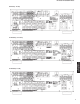
RX-V559/HTR-5950/DSP-AX559 ■ REAR PANELS RX-V559 (U, C models) RX-V559 (R model) RX-V559/HTR-5950/ DSP-AX559 RX-V559 (T model) 5
RX-V559/HTR-5950/DSP-AX559 RX-V559 (K model) RX-V559/HTR-5950/ DSP-AX559 RX-V559 (A model) RX-V559 (G, E models) 6
RX-V559/HTR-5950/DSP-AX559 RX-V559 (L model) HTR-5950 (U, C models) RX-V559/HTR-5950/ DSP-AX559 HTR-5950 (T model) 7
RX-V559/HTR-5950/DSP-AX559 HTR-5950 (A model) RX-V559/HTR-5950/ DSP-AX559 DSP-AX559 (J model) 8
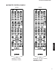
RX-V559/HTR-5950/DSP-AX559 ■ REMOTE CONTROL PANELS RAV322 RAV323 RX-V559/HTR-5950/ DSP-AX559 RX-V559 (U, C models) HTR-5950 (U, C models) RX-V559 (R, T, K, A, G, E, L models) HTR-5950 (T, A models) DSP-AX559 (J model) 9
RX-V559/HTR-5950/DSP-AX559 ■ SPECIFICATIONS / 参考仕様 ■ Audio Section / オーディオ部 RX-V559/HTR-5950/ DSP-AX559 Minimum RMS Output Power (Power Amp. Section) / 定格出力 (パ ワーアンプ部) [RX-V559] (20 Hz to 20 kHz, 0.06 % THD, 8 ohms) FRONT L/R ................................................................. 95 W + 95 W CENTER ................................................................................. 95 W SURROUND L/R ........................................................ 95 W + 95 W SURROUND BACK ...............
RX-V559/HTR-5950/DSP-AX559 • DIMENSIONS / 寸法図 * Specifications are subject to change without notice due to product improvements. RX-V559 DSP-AX559 22 (7/8") Manufactured under license from Dolby Laboratories. “Dolby”, “Pro Logic”, and the double-D symbol are trademarks of Dolby Laboratories. HTR-5950 393.2 (15-1/2") 350.2 (13-13/16") Manufactured under license from Digital Theater Systems, Inc. “DTS”, “DTS-ES”, “NEO:6”, and “DTS 96/24” are trademarks of Digital Theater Systems, Inc.
MANUAL SETUP BASIC SETUP CATEGORY 3 OPTION MENU 2 INPUT MENU 1 SOUND MENU MAIN MENU • Set Menu Table / セットメニュー B) C) D) E) (U model) PARAM. INI MULTI ZONE SET XM RADIO SET MEMORY GUARD A) DISPLAY SET B) INPUT MODE C) INPUT RENAME D) VOLUME TRIM A) I/O ASSIGNMENT G) AUDIO SET F) DYNAMIC RANGE E) LFE LEVEL D) CENTER GEQ C) SP DISTANCE B) SPEAKER LEVEL A) SPEAKER SET SUB MENU SELECT MENU SP B XM DISPLAY XM ANTENNA SCROLL DIMMER VIDEO CONV.
RX-V559/HTR-5950/DSP-AX559 ■ INTERNAL VIEW • RX-V559, DSP-AX559 1 2 3 4 5 6 7 8 9 0 A C H G B F E 1 OPERATION (4) P.C.B. 2 FUNCTION (2) P.C.B. 3 FUNCTION (3) P.C.B. (R, L models) 4 DSP P.C.B. 5 MAIN (5) P.C.B. 6 MAIN (4) P.C.B. 7 VIDEO P.C.B. 8 Tuner 9 FUNCTION (1) P.C.B. 0 MAIN (1) P.C.B. A FUNCTION (4) P.C.B. B MAIN (2) P.C.B. C Power Transformer D OPERATION (5) P.C.B. E OPERATION (1) P.C.B. F OPERATION (6) P.C.B. G OPERATION (3) P.C.B. H OPERATION (2) P.C.B.
RX-V559/HTR-5950/DSP-AX559 RX-V559/DSP-AX559 ■ DISASSEMBLY PROCEDURES / 分解手順 (Remove parts in the order as numbered.) Disconnect the power cable from the AC outlet. (番号順に部品を取り外してください。) AC電源コンセントから、電源コードを抜いてください。 1. Removal of Top Cover a. Remove 4 screws (1), 5 screws (2) and 1 screw (3). (Fig. 1) b. Slide the Top Cover rearward to remove it. (Fig. 1) 1. トップカバーの外し方 a. 1のネジ4本、2のネジ5本、3のネジ1本を外します。 (Fig. 1) b. トップカバーを後方へスライドさせ、取り外します。 (Fig. 1) 2. Removal of Front Panel Unit a. Remove 2 Knobs. (Fig. 1) b.
RX-V559/HTR-5950/DSP-AX559 5. a. b. c. d. Removal of FUNCTION (1) P.C.B. Remove 2 screws (9). (Fig. 2) Remove 8 screws (0). (Fig. 4) Remove CB200-202, CB204, CB206 and CB207. (Fig. 2) Remove the FUNCTION (1) P.C.B.. (Fig. 2) 5. FUNCTION(1)P.C.B.の外し方 a. 9のネジ2本を外します。(Fig. 2) b. 0のネジ8本を外します。(Fig. 4) c. CB200∼202、CB204、CB206、CB207を外します。 (Fig. 2) d. FUNCTION(1)P.C.B.を取り外します。(Fig. 2) 6. Removal of DSP P.C.B. a. Remove 2 screws (A). (Fig. 2) b.
RX-V559/HTR-5950/DSP-AX559 HTR-5950 When checking the P.C.B.: • Put a Cloth over the equipment. Put the P.C.B.s together with the Heat Sink upright on the Cloth and check them. (Fig. 6) • Reconnect all cables (connectors) that have been disconnected. • When connecting the flat cable, use care for the polarity. • The P.C.B. removed from the chassis does not work because its grounding is loose. Be sure to connect the ground of Rear Panel, MAIN (1) P.C.B. (G1001) and OPERATION (4) P.C.B.
RX-V559/HTR-5950/DSP-AX559 4. Removal of DSP P.C.B. a. Remove 2 screws (8). (Fig. 2) b. Remove 7 screws (U, C models) / 6 screws (T, A models) (9). (Fig. 4) c. Remove CB2-4, CB9 and CB57. (Fig. 2) d. Remove the DSP P.C.B.. (Fig. 2) 5. a. b. c. b. 6. a. b. c. Removal of FUNCTION (2) P.C.B. Remove 1 push rivet (B). (Fig. 3) Remove 5 screws (C). (Fig. 4) Remove the FUNCTION (2) P.C.B.. (Fig. 3) 7. Removal of TUNER a. Remove 3 screws (D). (Fig. 4) b. Remove the TUNER. (Fig. 5) Removal of VIDEO P.C.B.
RX-V559/HTR-5950/DSP-AX559 ■ SELF DIAGNOSIS FUNCTION (DIAG)/自己診断機能(ダイアグ) This unit has self diagnosis functions that are intended for inspection, measurement and location of faulty point. There are 23 DIAG menu items, each of which has submenu items. Listed in the table below are menu items and sub-menu items. Note that not all menu items listed will apply to the models covered in this service manual. No.
RX-V559/HTR-5950/DSP-AX559 • Starting DIAG ● ダイアグの起動 Press the “MASTER ON/OFF” (RX-V559/DSP-AX559 models) / “STANDBY/ON” (HTR-5950 model) key while simultaneously pressing those two keys of the main unit as indicated in the figure below. 本体の下図に示すキーを同時に押しながら “MASTER ON/OFF” キーを押すと、ダイアグが起動します。 Keys of main unit / 本体キー Turn on the power while pressing these keys.
RX-V559/HTR-5950/DSP-AX559 • Display provided when DIAG started ● ダイアグ起動時の表示 When the monitor is connected, DIAGNOSTIC MENU appears on its screen as shown in the figure. On the FL display of the main unit, an opening message (including the version and the protection history) appears for a few seconds followed by the diagnostic menu display (1. ANALOG BYPASS). モニターを接続してある場合は、モニターの画面に図のようにダ イアグメニューが表示されます。 本体FLディスプレイには、オープニング(プロテクション履歴/ バージョン)が表示され、数秒後にダイアグメニュー表示(1 . ANALOG BYPASS)となります。 1.BYPASS 2.
RX-V559/HTR-5950/DSP-AX559 The protection function worked due to the temperature limit being exceeded. Causes could be poor ventilation or a defect related to the thermal sensor. If the power is turned on with the abnormality unsolved, the protection function works in about 1 second to turn off the power. TMP PRT:000 A For detection of each protection function (except I-PROTECT) , refer to DIAG MENU No.10 AD DATA.
RX-V559/HTR-5950/DSP-AX559 Keys of main unit / 本体キー DIAG menu selection SUB-MENU selection ダイアグメニューの選択 サブメニューの選択 Reverse Forward Reverse Forward 逆送り 順送り 逆送り 順送り U, C models Reverse Forward 逆送り 順送り R, T, K, A, G, E, L, J models RX-V559/DSP-AX559 models Reverse Forward Reverse Forward Reverse Forward 逆送り 順送り 逆送り 逆送り 順送り U, C models 順送り T, A models HTR-5950 model • Functions in DIAG mode ● ダイアグ中の機能 In addition to the DIAG menu items, functions as listed below are available.
RX-V559/HTR-5950/DSP-AX559 • Details of DIAG menu ● ダイアグメニュー詳細 1. BYPASS 1. BYPASS Using the sub-menu, it is possible to select analog bypass output or DSP bypass output. サブメニューによりANALOG BYPASS/DSP BYPASSが選択 可能です。 ANALOG BYPASS ANALOG BYPASS 1.ANALOG BYPAS Reference data INPUT: DVD ANALOG SUBWOOFER OUTPUT: 50 Hz, Others: 1 kHz Input level Volume Both ch, -20 dBm +6.0 dB SPEAKERS OUT FRONT L/R +13.
RX-V559/HTR-5950/DSP-AX559 2. RAM THROUGH 2. RAM THROUGH Using the sub-menu, it is possible to select margin output or full-bit output. サブメニューによりMARGIN/Full Bitが選択可能です。 RAM MARGIN Following head margin is reserved. RAM MARGIN 以下のヘッドマージンを取ります。 FRONT CENTER SURROUND SURROUND BACK SUBWOOFER +15.0 dB +13.5 dB +9.0 dB +7.5 dB +21.0 dB 2.RAM MARGIN Reference data INPUT: DVD ANALOG SUBWOOFER OUTPUT: 50 Hz, Others: 1 kHz Input level Volume Both ch, -20 dBm +6.0 dB SPEAKERS OUT FRONT L/R +13.
RX-V559/HTR-5950/DSP-AX559 3. PRO LOGIC 3. PRO LOGIC Dolby PRO LOGIC is applied to input stereo source. 入力2ch信号にDolby PRO LOGIC処理を行います。 3.PRO LOGIC Reference data INPUT: DVD ANALOG SUBWOOFER OUTPUT: 50 Hz, Others: 1 kHz Input level Volume Each ch, -20 dBm +6.0 dB Both ch, -20 dBm +6.0 dB SPEAKERS OUT SUBWOOFER CENTER SURROUND L/R SURROUND BACK L/R OUTPUT FRONT L/R -∞ +16.5 dBm +13.5 dBm -20.
RX-V559/HTR-5950/DSP-AX559 4.FRNT:SML 0dB 4.CENTER:NONE 4.LFE/B:FRNT 4.Pres Mix:5ch 4.Front GAIN 1 4.Front GAIN 2 4.SURR B check Reference data INPUT: DVD ANALOG (Both ch) SUBWOOFER OUTPUT: 50 Hz, Others: 1 kHz Input level 1 FRONT: SML 0dB 2 CENTER: NONE Both ch, -20 dBm Both ch, -20 dBm +6.0 dB +13.5 dBm +13.5 dBm +13.5 dBm +13.5 dBm +6.0 dB +10.5 dBm -∞ +13.5 dBm +13.5 dBm +5.5 dBm +2.0 dBm LFE/B: FRNT (1 kHz) LFE/B: FRNT (50 Hz) Both ch, -20 dBm Both ch, -20 dBm +6.0 dB -∞ +13.5 dBm +13.
RX-V559/HTR-5950/DSP-AX559 5. XCH INPUT 5. XCH INPUT The signal input through the multi ch input is output. The speaker impedance can be selected. マルチCH入力された信号が出力されます。 6オーム、8オームが選択されます。 XCH INPUT_6 (ohms) XCH INPUT_6(ohms) 5.XCH INPUT_6 Reference data INPUT: MULTI CH INPUT SUBWOOFER OUTPUT: 50 Hz, Others: 1 kHz Input level Volume Both ch, -20 dBm +6.0 dB FRONT L/R +13.5 dBm SPEAKERS OUT SUBWOOFER CENTER SURROUND L/R SURROUND BACK L/R OUTPUT +13.5 dBm XCH INPUT_8 (ohms) +13.5 dBm -∞ -10.
RX-V559/HTR-5950/DSP-AX559 7. DISPLAY CHECK 7. DISPLAY CHECK This program is used to check the FL display section and video control section. The display condition varies as shown below according to the sub-menu operation. The signal route is STRAIGHT.
RX-V559/HTR-5950/DSP-AX559 8. MANUAL TEST 8. MANUAL TEST The test noise based THX is output to the channel specified by the sub-menu from the DSP. The noise frequency for LFE is 35 to 250 Hz. Other than that, the center frequency is 800 Hz. DSPからサブメニューで指定したチャンネルへTHX準拠のテス トノイズを出力します。 LFE用のノイズ周波数は35∼250 Hz、それ以外は中心周波数 800 Hzとなります。 8.TEST ALL 8.TEST FRNT L 8.TEST CENTER 8.TEST SURR R 8.TEST SB R Not applied to these models. このモデルには適用されません。 8.TEST FRNT R Not applied to these models.
RX-V559/HTR-5950/DSP-AX559 • PRESET STATIONS / プリセット局 STATION PAGE NO. 1 2 A/C/E FM FACTORY PRESET DATA (MHz) U, C 87.5 90.1 R, T, K, A, G, E, L 87.50 90.10 J 76.0 83.0 3 4 5 95.1 98.1 107.9 95.10 98.10 108.00 84.0 86.0 90.0 6 7 8 88.1 106.1 107.9 88.10 106.10 108.00 78.0 88.0 82.1 STATION PAGE NO.
RX-V559/HTR-5950/DSP-AX559 IMP SW/POWER LIMIT (impedance/power limiter detection) IMP: Not applied to these models. PL: Power limiter detection value The voltage value of pin No. 123 of IC2 is displayed, using 5V/256 as standard. The port (No. 6) output is controlled by using the input voltage value of pin No. 123 of IC2.
RX-V559/HTR-5950/DSP-AX559 11. VIDEO 11. VIDEO The image signal is converted and output as follows. I2C Perform the read/write check between the microprocessor and ADV7180 (IC411) as well as ADV7172 (IC412).
RX-V559/HTR-5950/DSP-AX559 DIGITAL THR Y/C DIGITAL THR Y/C DIGITAL Y/C Component Component DIGITAL THR Y/C VIDEO IC408 LC74781 VIDEO IC411 ADV7180 VIDEO IC412 ADV7172 S-Video S-Video Composite Composite ANALOG BYPASS ANALOG BYPASS ANALOG BYPASS Component Component ANALOG BYPASS VIDEO IC408 LC74781 VIDEO IC411 ADV7180 VIDEO IC412 ADV7172 S-Video S-Video Composite Composite RX-V559/HTR-5950/ DSP-AX559 TEST PATTERN TEST PATTERN TEST PATTERN VIDEO IC408 LC74781 S-Video Composite
RX-V559/HTR-5950/DSP-AX559 LOOP BACK CVBS Not applied to these models. LOOP BACK CVBS このモデルには適用されません。 LPBK CVBS OK VIDEO IC408 LC74781 VIDEO IC411 ADV7180 S-Video Component Component LOOP BACK CVBS VIDEO IC412 ADV7172 TEST PATTERN IC713 TEST Pattern (480i/576i) S-Video Composite Composite Connected by RCA cable LOOP BACK Y/C Not applied to these models.
RX-V559/HTR-5950/DSP-AX559 12. XM STATUS (U, C models) 12. XM STATUS(U、C models) Perform the output check of XM Radio Antenna connected to the XM terminal. XM端子に接続された、XM Radio Antennaの出力チェックを行 います。 1k -1dB/44.1k The test tone (1kHz, -1dB/44.1kHz) is output. 1k -1dB/44.1k テストトーン (1kHz、-1dB/44.1kHz)を出力します。 1k - 1dB/44 1k -61dB/44.1k The test tone (1kHz, -61dB/44.1kHz) is output. 1k -61dB/44.1k テストトーン (1kHz、-61dB/44.1kHz)を出力します。 1k -61dB/44 Mute /44.1k Nothing is output. Mute /44.
RX-V559/HTR-5950/DSP-AX559 Mute /32k Nothing is output. Mute /32k 何も出力されません。 Mute XM Tone/32k The XM tone (32kHz) is output. /32 XM Tone/32k XMトーン(32kHz)を出力します。 XM Tone/32 ISO Tone/32k The ISO tone (32kHz) is output. ISO Tone/32k ISOトーン(32kHz)を出力します。 ISO Tone/32 XM/DT Bus Power: OFF The power of XM module is turned off. XM/DT Bus Power: OFF XMモジュールの電源をOFFします。 Bus Power:OFF 13. iPod 13. iPod RX-V559/HTR-5950/ DSP-AX559 This menu is used to test the DOCK connector without the iPod itself.
RX-V559/HTR-5950/DSP-AX559 16. IF STATUS (Input function status) 16. IF STATUS Using the sub-menu, the status data is displayed one after another in the hexadecimal notation. During signal processing, the status before execution of this menu is maintained. サブメニュー操作により、以下のステータス情報を順次16進数で 表示します。信号処理は、本メニュー実行前の状態を維持しま す。 ※図中の数値は参考例です。 * Numeric values in the figure example are for reference.
RX-V559/HTR-5950/DSP-AX559 <5th byte> / <第5バイト> Signal processing status information / 信号処理ステータス情報 bit bit 7 bit 6 bit 5 bit 4 bit 3 bit 2 bit 1 bit 0 Fs (kHz) Digital mute – 6.1 (7.1) processing Analog mute – PCM through – dts analog mute DMD: Decoder mode information Not applied to these models. DMD:デコーダー情報 このモデルには適用されません。 DMD:03C00000 DIF: DIR information Not applied to these models. DIF:DIR情報 このモデルには適用されません。 DIF:0001000600 PC: Preamble C information Not applied to these models.
RX-V559/HTR-5950/DSP-AX559 DGI: Digital information Not applied to these models. DGI:DIGITAL系情報 このモデルには適用されません。 DGI:EE6464F95E 17. DSP BUS CHECK 17. DSP BUS CHECK This menu is used to self-diagnose whether or not the bus connection for the TI (DA70Y) and the external ROM/RAM is made properly. When no error is detected, "NoEr" appears on display. TI(DA70Y) と外付けROM/RAMとのバス接続の正否を自己診断 します。 エラーが検出されなかった場合は、“NoEr”と表示されます。 TI BUS:NoEr No error detected.
RX-V559/HTR-5950/DSP-AX559 21. SOFT SW 21. SOFT SW Note) Changing the function setting may hinder the proper operation. 注)機能設定を変更した場合、正常に動作しないことがありま す。 This menu is used to switch the function settings on P.C.B. through the software so as to activate the product. The protection function follows the P.C.B. settings. When connected to AC or in the maker preset state, the unit is initialized to the P.C. B. setting. Display of each function after initialization varies depending on settings on P.C.B.
RX-V559/HTR-5950/DSP-AX559 ZONE2: NOT or EXIST can be selected. (SW MODE: Selectable when FNC has been selected.) ZONE2:NOTまたはEXISTを選択できます。(SW MODE: FNC時選択できます。) 21.ZONE2:EXIST AAC: NOT or EXIST can be selected. (SW MODE: Selectable when FNC has been selected.) 21.AAC TUNER: NOT or EXIST can be selected. (SW MODE: Selectable when FNC has been selected.) AAC:NOTまたはEXISTを選択できます。 (SW MODE:FNC 時選択できます。) :NOT TUNER:NOTまたはEXISTを選択できます。(SW MODE: FNC時選択できます。) 21.
RX-V559/HTR-5950/DSP-AX559 22. SOFTWARE VERSION 22. SOFTWARE VERSION The version, checksum and the port specified by the microprocessor are displayed. The signal is processed using EFFECT OFF. The checksum is obtained by adding the data at every 16 bits for each program area and expressing the result as a 4-figure hexadecimal data. ソフトウェアのバージョン、チェックサム、マイコンの指定ポー トを表示します。 信号はエフェクトOFFです。チェックサムは、プログラムエリア 別にデータを16ビットごとに加算していき、4桁の16進データ で現したものです。 * Numeric values in the figure example are for reference.
RX-V559/HTR-5950/DSP-AX559 ■ AMP ADJUSTMENT / アンプ部調整 Confirmation of Idling Current of MAIN (1) P. C. B. メイン(1) 基板のアイドリング電流の確認 • Right after power is turned on, confirm that each measured voltage across the terminals of R1149 (FRONT Lch), R1150 (FRONT Rch), R1153 (CENTER), R1154 (SURROUND Lch), R1152 (SURROUND Rch), R1151 (SURROUND BACK) is between 0.1 mV and 10.0 mV. ● 電源投入直後、R1149(FRONT Lch)、R1150(FRONT Rch) 、R1153 (CENTER) 、R1154 (SURROUND Lch) 、 R1152(SURROUND Rch)、R1151(SURROUND BACK) の端子間電圧を測定し、0.
RX-V559/HTR-5950/DSP-AX559 RX-V559/DSP-AX559 ■ DISPLAY DATA ● V3000 : HNA-17MM03T (WG474000) } 1 PATTERN AREA ● PIN CONNECTION Pin No. 69 68 67 66 65 64 63 62 61 60 59 58 57 56 55 54 53 52 51 50 49 48 47 46 45 44 43 42 41 40 39 38 37 36 35 Connection F2 F2 NP NP P1 P2 P3 P4 P5 P6 P7 P8 P9 P10 P11 P12 P13 P14 P15 P16 P17 P18 P19 P20 P21 P22 P23 P24 P25 P26 P27 P28 P29 P30 P31 Pin No.
RX-V559/HTR-5950/DSP-AX559 ● ANODE CONNECTION 17G 16G 15G 14G 13G~1G S1 S1 1-1 1-1 P2 W1 2-1 2-1 P3 W2 3-1 3-1 P4 4g 4-1 4-1 P5 1a 5-1 5-1 P6 1b 1-2 1-2 P7 1c 2-2 2-2 P8 1d 3-2 3-2 P9 1e 4-2 4-2 P10 1f 5-2 5-2 P11 1g 1-3 1-3 P12 2a 2-3 2-3 P13 2b 3-3 3-3 P14 2c 4-3 4-3 P15 2d 5-3 5-3 P16 2e 1-4 1-4 P17 2f 2-4 2-4 P18 2g 3-4 3-4 P19 3g 4-4 4-4 P20 3b 5-4 5-4 P21 3a 1-5 1-5 2-5 2-5 P1 P22 R1 3-5 3-5 P24 R2 4-5 4
RX-V559/HTR-5950/DSP-AX559 HTR-5950 ■ DISPLAY DATA ● V3000 : 17-BT-26GNK (WG473900) } 1 PATTERN AREA ● PIN CONNECTION Pin No. 69 68 67 66 65 64 63 62 61 60 59 58 57 56 55 54 53 52 51 50 49 48 47 46 45 44 43 42 41 40 39 38 37 36 35 Connection F2 NX NP NP P1 P2 P3 P4 P5 P6 P7 P8 P9 P10 P11 P12 P13 P14 P15 P16 P17 P18 P19 P20 P21 P22 P23 P24 P25 P26 P27 P28 P29 P30 P31 Pin No.
RX-V559/HTR-5950/DSP-AX559 ● ANODE CONNECTION 1G~13G 14G 15G 16G 1P 1-1 1-1 S2 S1 2P 2-1 2-1 S26 S6 3P 3-1 3-1 S27 S7 4P 4-1 4-1 S22 S8 5P 5-1 5-1 1a S9 6P 1-2 1-2 1b S10 7P 2-2 2-2 1c S11 8P 3-2 3-2 1d S12 9P 4-2 4-2 1e 10P 5-2 5-2 1f 11P 1-3 1-3 1g 12P 2-3 2-3 2a 13P 3-3 3-3 2b 14P 4-3 4-3 2c 15P 5-3 5-3 2d 16P 1-4 1-4 2e 17P 2-4 2-4 2f 18P 3-4 3-4 2g 19P 4-4 4-4 S23 20P 5-4 5-4 S24 21P 1-5 1-5 S25 22P 2-5 2
RX-V559/HTR-5950/DSP-AX559 ■ IC DATA : M30625MHP-A98GP (DSP P.C.B.
RX-V559/HTR-5950/DSP-AX559 IC2 No.
RX-V559/HTR-5950/DSP-AX559 RX-V559/HTR-5950/ DSP-AX559 IC2 No.
RX-V559/HTR-5950/DSP-AX559 IC2 : M30625MHP-A98GP (DSP P.C.B.) Microprocessor No. 106 107 108 109 110 111 112 113 114 Port Name P05/D5 P04/D4 P03/D3 P02/D2 P01/D1 P00/D0 P117 P116 P115 115 P114 116 P113 117 P112 118 P111 119 P110 120 121 122 123 124 125 126 127 128 P107/AN7/KI3 P106/AN6/KI2 P105/AN5/KI1 P104/AN4/KI0 P103/AN3 P102/AN2 P101/AN1 Avss P100/AN0 Terminal Name DTEV CKZ2 DTZ2 N.C. N.C.
RX-V559/HTR-5950/DSP-AX559 : LC89057W-VF4-E (DSP P.C.
RX-V559/HTR-5950/DSP-AX559 IC56 Name RXOUT RX0 RX1 RX2 RX3 DGND DVDD RX4 RX5/VI RX6/UI DVDD DGND LPF ACDD AGND RMCK RBCK DGND DVDD RLRCK RDATA SBCK SLRCK SDIN DGND DVDD XMCK XOUT XIN DVDD DGND EMPHA/UO AUDIO/VO CKST INT RERR DO DI CE CL XMODE DGND DVDD TMCK/PIO0 TMCK/PIO1 TLRCK/PIO2 TLRCK/PIO3 TXO/PIOEN I/O O Is I Is Is Is Is Is O O O/I O/I O O O Is O O I I/O I/O I/O I/O O O Is Is Is Is I/O I/O I/O I/O O/I Function Input bi-phase selection data output pin TTL-compatible digital data input pin Coa
RX-V559/HTR-5950/DSP-AX559 IC60 : D70YE101RFP250 (DSP P.C.B) Decoder/Post Processor 108 107 106 105 104 103 102 101 100 99 98 97 96 95 94 93 92 91 90 89 88 87 86 85 84 83 82 81 80 79 78 77 76 75 74 73 SPI0_CLK/I2C0_SCL SPI0_SCS/I2C1_SCL Vss SPI0_ENA/I2C1_SDA EM_OE DVDD EM_RW CVDD EM_CS[2] Vss EM_RAS EM_CS[0] EM_BA[0] Vss EM_BA[1] EM_A[10] DVDD EM_A[0] CVDD EM_A[1] EM_A[2] Vss EM_A[3] CVDD EM_A[4] EM_A[5] Vss DVDD EM_A[6] EM_A[7] Vss CVDD EM_A[8] EM_A[9] EM_A[11] DVDD * No replacement part available.
RX-V559/HTR-5950/DSP-AX559 IC60 SIGNAL NAME Ground(Vss) AHCLKX0/AHCLKX2 AMUTE0 AMUTE1 AHCLKX1 Ground(Vss) ACLKX1 Core Supply (CVpp) ACLKR1 IO Supply (DVpp) AFSX1 AFSR1 Ground(Vss) RESET Ground(Vss) Core Supply (CVpp) CLKIN Ground(Vss) TMS Core Supply (CVpp) TRST OSCVss OSCIN OSCOUT OSCVpp Ground(Vss) PLLHV TDI TDO Ground(Vss) IO Supply (DVpp) EMU[0] Core Supply (CVpp) EMU[1] TCK Ground(Vss) EM_CAS EM_WE EM_WE_DQM[0] Ground(Vss) EM_D[7] IO Supply (DVpp) EM_D[6] Core Supply (CVpp) EM_D[5] EM_D[4] Ground(Vss
RX-V559/HTR-5950/DSP-AX559 IC60 RX-V559/HTR-5950/ DSP-AX559 PIN NO. 56 57 58 59 60 61 62 63 64 65 66 67 68 69 70 71 72 73 74 75 76 77 78 79 80 81 82 83 84 85 86 87 88 89 90 91 92 93 94 95 96 97 98 99 100 101 102 103 104 105 106 107 108 109 110 56 : D70YE101RFP250 (DSP P.C.
RX-V559/HTR-5950/DSP-AX559 IC60 PIN NO. 111 112 113 114 115 116 117 118 119 120 121 122 123 124 125 126 : D70YE101RFP250 (DSP P.C.
RX-V559/HTR-5950/DSP-AX559 ■ PIN CONNECTION DIAGRAM • ICs BD3816K1 BD3841FS 64 TC74HC4051AF TC74HC4052AF TC74HC4053AF NJM2581M 41 65 LA7106M-TLM-E PCM1780DBQR PCM1781DBQR PCM1803DBR F2602E-01 YAC523-EVR2 40 17 36 48 13 1 25 8 7 14 1 24 16 32 80 25 37 1 1 16 1 12 24 BD3816K1 LA73050-TLM-E LC72722PM LC89057W-VF4A-E 24 LM61CIZ THERMAL 13 25 12 36 1 18 12 36 24 +VS VOUT GND IN OUT COM 1 M30625MHP-A98GP 102 103 37 1 M66003-0131FP 48 65 64 NE5532DR OP AMP 48
RX-V559/HTR-5950/DSP-AX559 SN74LV157APWR SN74LVU04APWR SN74LV245APWR TRAN TC4013BP FF TC74VHCU04FT INVER W9816G6CH-7 SDRAM 50 YAC520-EE2 26 10 14 10 7 7 20 14 20 1 1 1 1 25 1 ADV7180 ADV7172 64 49 48 1 48 16 33 S29AL004D70TF1020 37 12 17 48 24 25 25 13 32 1 36 1 24 • Diodes 1N4002S RB441Q-40 T-77 1SS133,176 RB441Q-40 T-77 1SS270A 1SS355 1SS380 1T2 MTZJ13A 13V MTZJ15A 15V MTZJ15B 15V Anode MTZJ2.4B 2.4V MTZJ27B 27V MTZJ30A 30V MTZJ5.1C 5.1V Cathode D2SBA20 1.
RX-V559/HTR-5950/DSP-AX559 RX-V559/HTR-5950/ DSP-AX559 MEMO 60
A B C D E F G H I J RX-V559/DSP-AX559/HTR-5950 1 ■ BLOCK DIAGRAMS AUDIO BLOCK DIAGRAM • See page 81-83 → SCHEMATIC DIAGRAM D70YE001RFP250 Decoder / Post Prosessor IC60 DIGITAL AXR0[11] RX4 DTV/CBL R, T, K, A, G, E, L, J models 6 DVD Buffer SN74LVU04APWR *VDD=5V IC52 J206 21 9 8 RX5 RDA 130 1 MD/CD-R Post Prosessor RX3 8 2 131 Decoder DVD AXR0[4] RX2 5 AXR0[3] AXR0[2] AXR0[1] AXR1[3] AXR0[0] U, C models 117 116 115 113 6 FL/FR 11 C/SW 12 SL/SR 13 SB RXOUT 1
A B C D E F G H I J RX-V559/DSP-AX559/HTR-5950 1 VIDEO BLOCK DIAGRAM OUTPUT AMP LA73050 IC401 BYPASS 3 Y 8 S-Detector Y IC403 74HCU04 IC406 47, 48 0dB DVR 4 VIDEO VIA VIB VIC 4 Y FUNCTION Pb/Cb /INTCNV • See page 84 → SCHEMATIC DIAGRAM • See page 88 → SCHEMATIC DIAGRAM 13 12 D/A Encoder ADV7172 IC412 CVBS 12 28 CVBS 25 24 Y C 35, 33, 29 Y, Cb, Cr Y 15 14 C 17 15 22 6dB 15, 13, 11 MONITOR OUT Y Pb/Cb Pr/Cr COMP0 COMP1 Y Cb Cr Y Cb Cr Input Selector 74HC405
A B C D E F G H I J RX-V559/DSP-AX559/HTR-5950 1 MODEL DETECT • See page 81-83 → SCHEMATIC DIAGRAM 6 TONE CONTROL/ DSP PROGRAM SW302 60/ 62 POWER SAVE C1104 C1106 D133 C1105 /4ohms +BL G -BL -30V 7 Microprocessor M30627 IC2 56 + DSP FL2 iPod/Net-module 34/ 35 97 +12V IC104 XM 69/ 84/ 86/ 88/ 89/ 117 Zone2 POWER SW SW303 RDS/OSD C1083 83/ 90- 95 TUNER MAIN POWER SW SW304 -VP Q1068 • See page 87 → SCHEMATIC DIAGRAM FL1 8-10/ 15/ 16/ 23/ 24/ 26- 31 12/ 42- 45 RX-V55
A B C D E F G H I J RX-V559/DSP-AX559/HTR-5950 ■ PRINTED CIRCUIT BOARDS FUNCTION (1) FUNCTION (1) (CB200) (CB202) RM/ST TMT SDRN SDTN SDRP SDTP /HP MTFS MTSW CKEV CKZ2 -12 CKEX DSP P.C.B.
A B C D E F G H I J RX-V559/DSP-AX559/HTR-5950 1 DSP P.C.B. (Side B) 2 Lead Free Solder Used RX-V559/DSP-AX559 model 3 4 5 6 • Semiconductor Location Ref no. Location Ref no.
A B C D E F G H I J RX-V559/DSP-AX559/HTR-5950 ADR L E SW SL E E XMR E IPR ADL E R C E SR SB XML REMsense IPL DSP FUNCTION (1) P.C.B.
A B C D E F G H I J RX-V559/DSP-AX559/HTR-5950 1 FUNCTION (1) P.C.B. (Side B) Lead Free Solder Used 2 RX-V559/DSP-AX559 models 3 65 64 4 32 17 1 16 80 1 41 40 4 1 24 25 5 8 4 1 5 8 RX-V559/DSP-AX559 models 5 32 1 17 16 • Semiconductor Location 6 12 1 13 24 Ref no. Location Ref no.
A B C D E F G H I J RX-V559/DSP-AX559/HTR-5950 1 COMPONENT VIDEO A DVD / B DTV/CBL D4 VIDEO (J model) DVD A FUNCTION (2) P.C.B.
A B C D E F G H I J RX-V559/DSP-AX559/HTR-5950 1 2 FUNCTION (2) P.C.B. (Side B) Lead Free Solder Used 3 9 4 16 8 1 8 7 1 16 8 9 9 8 16 1 14 1 8 7 14 1 5 9 8 16 1 • Semiconductor Location Ref no. Location Ref no.
A B C D E F G H I J RX-V559/DSP-AX559/HTR-5950 1 +5M MASTER F2 F1 RX-V559/DSP-AX559 OPERATION (1) P.C.B. (Side A) 2 MG MPSW ZONE ZONE 2 CONTROL ON/OFF HPR HPE HPL MG /HP 4 VP MG +5S +5M RM+ RM/PSW REM MASTER /BLK MG N.
A B C D E F G H I J RX-V559/DSP-AX559/HTR-5950 1 RX-V559/DSP-AX559 2 OPERATION (1) P.C.B. (Side B) Lead Free Solder Used 3 33 32 48 17 49 16 64 1 4 5 OPERATION (3) P.C.B. (Side B) Lead Free Solder Used • Semiconductor Location Ref no. Location Ref no.
A B C D E F G H I J RX-V559/DSP-AX559/HTR-5950 1 RX-V559/DSP-AX559 OPERATION (4) P.C.B. (Side A) OPERATION (5) P.C.B. (Side A) 2 to POWER TRANSFORMER FUNCTION (3) U, C, T, K, A, B, G, J models AC IN R, L models (W3005A, W3005B) VIDEO AUX 3 AUDIO 8 7 14 1 L R PORTABLE L VIDEO R 4 AXR E AXL VE AUX-V VE N.C N.C AC OUTLET 5 FUNCTION (1) (CB203) DSP (CB3) 7 72 E E S10 S10 PRY E E PDET +5M /RES 6 • Semiconductor Location Ref no. Location Ref no.
A B C D E F G H I J RX-V559/DSP-AX559/HTR-5950 1 RX-V559/DSP-AX559 2 OPERATION (4) P.C.B. (Side B) OPERATION (5) P.C.B. (Side B) Lead Free Solder Used Lead Free Solder Used 3 4 5 6 • Semiconductor Location Ref no. Location Ref no.
A B C D E F G H I RX-V559/DSP-AX559/HTR-5950 1 HTR-5950 OPERATION (1) P.C.B. (Side A) VP MG +5S +5M RM+ RM/PSW REM MASTER /BLK MG N.
A B C D E F G H I J RX-V559/DSP-AX559/HTR-5950 1 HTR-5950 OPERATION (1) P.C.B. (Side B) Lead Free Solder Used 2 33 32 48 17 49 16 64 1 3 4 5 OPERATION (3) P.C.B. (Side B) Lead Free Solder Used 6 • Semiconductor Location Ref no. Location Ref no.
A B C D E F G H I J RX-V559/DSP-AX559/HTR-5950 1 HTR-5950 OPERATION (4) P.C.B. (Side A) OPERATION (4) P.C.B. (Side B) Lead Free Solder Used AC IN to POWER TRANSFORMER 2 8 7 14 1 3 AC OUTLET S10 S10 PRY E E PDET +5M /RES E E 4 DSP MAIN (1) (CB3) (W1029) OPERATION (5) P.C.B. (Side A) 5 OPERATION (5) P.C.B. (Side B) Lead Free Solder Used VIDEO VIDEO AUX AUDIO L R PORTABLE • Semiconductor Location Ref no. Location Ref no. Location N.C N.
A B C D E F G H I J RX-V559/DSP-AX559/HTR-5950 1 SPEAKERS FRONT A/B + SURROUND L/R SURROUND CENTER BACK + – – + L R – – • Semiconductor Location + RX-V559/ DSP-AX559 models +18 E -18 E +10 E -10 +IPOD E E MAIN (2) (W1000B) REMOTE CONTROL OUT IN OUT Ref no. Location Ref no. Location (CB331) MAIN (1) P.C.B.
A B C D E F G H I J RX-V559/DSP-AX559/HTR-5950 1 2 MAIN (2) P.C.B. (Side A) Lead Free Solder Used MAIN (1) MAIN (1) (W1002A) VIDEO (W1001A) MAIN (1) 3 DSP (CB57) +18 E -18 E +10 E -10 +IPOD E E E E +XM +12 -12 PRV1 THM -5V N.C. +5V (CB401) (W1000A) IGND +5I XGND +5.3X XMPWR +3.3D +5D -12 +12 PRV2 1 4 1 4 1 4 1 4 4 MAIN (4) P.C.B. (Side A) Lead Free Solder Used MAIN (1) (CB115) MAIN (5) P.C.B.
A B C D E F G H I J RX-V559/DSP-AX559/HTR-5950 1 VIDEO VIDEO P.C.B.
A B RX-V559/DSP-AX559/HTR-5950 1 VIDEO P.C.B.
A B C D E F G H I J L K M N RX-V559/HTR-5950/DSP-AX559 SCHEMATIC DIAGRAMS DSP 1/3 1 DSP POINT A-1 Pin 18 of IC2 POINT B-2 1 / Pin7, 2 / Pin8 of CB3 2 3 to FUNCTION (1)_CB200 Page 84 C1 POWER ON (connect the power cable) IC1 : RH5RE58AA-T1-FA Voltage regulator 5.0 VIN -11.9 VOUT 2 4.9 3 RX-V559/DSP-AX559 models + – 5.0 Vref 4.3 1 0 0 0 0 0 4.9 4.9 4.9 5.0 0 0.1 0 5.0 D8 4.8 5.0 0 0 5.0 0 5.0 MICROPROCESSOR -11.9 4.9 0 4.9 0 4.9 0 0 0 0 0 5.
A B C D E F G H I J L K M N RX-V559/HTR-5950/DSP-AX559 DSP 2/3 1 DSP IC61, 62 : SN74AHCT1G32DCKR Single 2-input positive-OR gate 5.0 1 B 2 GND 3 5 4 Vcc 1A 1 14 Vcc 1B 2 13 4B 1Y 3 12 4A 2A 4 11 4Y 2B 5 10 3B 2Y 6 9 3A GND 7 8 3Y Y 0 3.3 3.3 3.1 A 5.0 0 3.3 5.0 0.9 3.3 3.1 0 0.1 0 100/16 3.1 3.2 100/16 1.3 100/16 0 1.3 0 2 3.3 no_use (HTR-5950 model) IC63 : SN74AHCT08PWR Quadruple 2-input positive-AND gates 0 3.1 0.1 3.
A B C D E F G H I J L K M N RX-V559/HTR-5950/DSP-AX559 DSP 3/3 1 Page 87 D2 Page 84 J8 to MAIN (2)_W1004 to FUNCTION (1)_CB202 DSP 2 DSP-AX559 8.8 RX-V559 HTR-5950 5.1 3 8.8 5.1 0 LC89057W-VF4A-E 0 3.3 3.3 1.7 0 3.3 11.8 0 0 0 2.5 0 0 2.5 0 5.0 3.3 0 2.5 0 2.5 0 0 0 2.5 4 5.0 0 0 ANALOG IN 2.5 1.3 2.5 1.7 2.5 1.7 5.0 LC89057W-VF4AD-E -11.9 2ch DAC FRONT L IC71-74, 75, 76 : NJM4565M Dual operatinonal amplifier 0 0 11.
A B C D E F G H I J L K M N RX-V559/HTR-5950/DSP-AX559 FUNCTION 65 GOUTFR 66 THGND 67 MUTE 68 CL 69 DA 70 AGND11 71 VEE 72 VCC 73 AGND12 to OPERATION (5)_W3007 74 ROUTA1 to DSP_CB56 to DSP_CB1 IC200 : BD3816K1 7-channel volume IC for 7-channel 75 ROUTA2 I4 76 ROUTB1 K7 HTR-5950: Page 86 77 ROUTB2 RX-V559/DSP-AX559: Page 85 C1 78 ROUTC1 Page 83 79 ROUTC2 B3 Page 81 80 AGND13 1 LOGIC REC A REC B REC C AGND1 1 64 VINFR INA1 2 63 GOUTFL BD3816K1 INA2 3 INB1 4 I
A B C D E F G H I J L K M N RX-V559/HTR-5950/DSP-AX559 OPERATION RX-V559/DSP-AX559 1 U, C, T, K, A, G, J models to POWER TRANSFORMER Page 84 J9 R, L models to FUNCTION (3)_W3005A,W3005B to POWER CABLE 2 5.2 VU99500 MA8091-M9.1V D3015 VU99500 MA8091-M9.1V VU99470 MA8082-H8.5V VU99500 MA8091-M9.1V VU99500 MA8091-M9.1V VU99500 MA8091-M9.1V VU99500 MA8091-M9.1V ~ 3 220K 5.0 ~ ~ ~ ~ ~ ~ AC7.9 ~ 4.9 0 5.0 5.0 ~ ~ ~ 0.2 5.0 0 0 -21.1 -21.
A B C D E F G H I J L K M N RX-V559/HTR-5950/DSP-AX559 OPERATION 1 HTR-5950 to TRANSFORMER 2 to POWER CABLE 220K B8 6800P 6800P Page 84 E7 FL DRIVER Page 81 5 to POWER TRANSFORMER to DSP_CB3 4 to FUNCTION (1)_CB203 3 PORTABLE OPERATION (5) 6 OPERATION (3) OPERATION (4) Page 87 7 H8 to MAIN (1)_W1029 OPERATION (1) Page 81 B5 to DSP_CB5 8 Page 84 E7 to FUNCTION (1)_CB205 OPERATION (6) IC301: M66003-0131FP FL display driver IC302 : TC4013BP Dual D-type flip fl
A B C D E F G H I J L K M N RX-V559/HTR-5950/DSP-AX559 MAIN 59.9 59.8 0 0.6 B9 1.1 0.6 0.1 -0.4 -1.0 1.0 -1.0 58.2 0.1 0.6 59.3 4.7/50 59.6 U, C, R, T, K, G, E, L models: 0 J model: 4700P 0 Over Voltage Protection 0 0 0 0 IC101: LM61CIZ Temperature sensor 0 58.8 1.1 1.1 58.2 0.1 0.6 4.7/50 0 -0.6 0.1 0 59.6 0.1 -0.4 0 0.1 0.6 59.3 0 -1.0 E8 59.9 0.1 0 59.9 1.1 0.1 0 1.1 3 U, C, R, T, K, G, E, L models: 0 J model: 0.01 0 -58.3 58.
A B C D E F G H I J L K M N RX-V559/HTR-5950/DSP-AX559 VIDEO 1 Page 87 Page 84 J9 H3 Page 84 to FUNCTION (2)_CB290 to MAIN (2)_W1006 C9 IC401 : LA73050-TLM-E Analog amplifier to FUNCTION (1)_CB201 2 IC402~404 : TC74HC4051AF Analog multiplexers/demultiplexers N.C. 1 36 N.C. N.C. 2 35 N.C. VIN1 3 DCCNT1 4 GND 5 4.9 1.9 6 VIN2 6dB 5.0 3.4 5.0 5.0 DR 3.
RX-V559/HTR-5950/DSP-AX559 ■ REPLACEMENT PARTS LIST • ELECTRICAL COMPONENT PARTS WARNING ● Components having special characteristics are marked s and must be replaced with parts having specifications equal to those originally installed. ● s印のある部分は、安全確保部品を示しています。部品の交換が必要な場合、パーツリストに記載されている部品を使用してください。 ● 部品価格ランクは、予告なく変更することがあります。 ABBREVIATIONS IN THIS LIST ARE AS FOLLOWS: : : : : : : : : : : : : : : : : : : : : : : : : : : : : : : : : : : : : : : : : : : : : : : : : : : : : : : : CHIP ALUMI.
RX-V559/HTR-5950/DSP-AX559 RX-V559/DSP-AX559 HTR-5950 P.C.B. DSP Ref. No. Part No.
RX-V559/HTR-5950/DSP-AX559 RX-V559/DSP-AX559 HTR-5950 P.C.B. DSP Part No.
RX-V559/HTR-5950/DSP-AX559 RX-V559/DSP-AX559 HTR-5950 P.C.B. DSP * * RX-V559/HTR-5950/ DSP-AX559 * * * * * * * * Ref. No. Part No.
RX-V559/HTR-5950/DSP-AX559 RX-V559/DSP-AX559 HTR-5950 P.C.B. DSP & P.C.B. FUNCTION Ref. No. * CB200 CB201 CB202 CB203 CB204 CB205 CB206 CB207 CB286-289 CB290 CB291 * * * * * * Description WG559700 WG559800 WA674700 WE436500 V3625700 R.CHP R.CHP R.CHP R.CHP R.CHP R.CHP R.CHP R.CHP R.CHP R.CAR.FP R.CHP R.CHP R.CHP R.CHP R.MTL.FLM R.CHP R.CHP R.MTL.FLM R.CHP R.CHP R.CHP R.CHP R.CHP R.CHP R.CAR.FP R.MTL.FLM R.CAR.FP R.MTL.FLM R.MTL.FLM R.CHP R.CHP R.CHP R.MTL.CHP R.MTL.CHP R.CHP CN.PHOTO CN.PHOTO RSNR.
RX-V559/HTR-5950/DSP-AX559 RX-V559/DSP-AX559 HTR-5950 P.C.B. FUNCTION RX-V559/HTR-5950/ DSP-AX559 * * Ref. No. Part No.
RX-V559/HTR-5950/DSP-AX559 RX-V559/DSP-AX559 HTR-5950 P.C.B. FUNCTION * * * * * * Part No.
RX-V559/HTR-5950/DSP-AX559 RX-V559/DSP-AX559 HTR-5950 P.C.B. FUNCTION RX-V559/HTR-5950/ DSP-AX559 * * * Ref. No. Part No.
RX-V559/HTR-5950/DSP-AX559 RX-V559/DSP-AX559 RX-V559/DSP-AX559 P.C.B. OPERATION Ref. No.
RX-V559/HTR-5950/DSP-AX559 RX-V559/DSP-AX559 HTR-5950 RX-V559/DSP-AX559 P.C.B. OPERATION & HTR-5950 P.C.B. OPERATION s s s s s s s s * RX-V559/HTR-5950/ DSP-AX559 s s * s * s * s * Ref. No. Part No.
RX-V559/HTR-5950/DSP-AX559 HTR-5950 HTR-5950 P.C.B. OPERATION * s s s s s s s Part No.
RX-V559/HTR-5950/DSP-AX559 RX-V559/DSP-AX559 HTR-5950 HTR-5950 P.C.B. OPERATION & P.C.B. MAIN Ref. No. * JK302 PJ300 PN331 Q3000-3001 Q3002 Q3003 Q3004-3005 Q3006 Q3007 Q3008 R3031 s RY301 ST300 ST316 ST318 SW300 SW301 SW302 SW304 SW306 SW309-319 SW321-324 * s T3000 * s T3000 TE300 TE300 TE300 U3000 * V3000 RX-V559/HTR-5950/ DSP-AX559 * * * * * Part No.
RX-V559/HTR-5950/DSP-AX559 RX-V559/DSP-AX559 HTR-5950 P.C.B. MAIN * * * * * * * Part No.
RX-V559/HTR-5950/DSP-AX559 RX-V559/DSP-AX559 HTR-5950 P.C.B. MAIN s * s RX-V559/HTR-5950/ DSP-AX559 s s s s * * * Ref. No. Part No.
RX-V559/HTR-5950/DSP-AX559 RX-V559/DSP-AX559 HTR-5950 P.C.B. MAIN s s s s s s s s s s s s s s s Part No.
RX-V559/HTR-5950/DSP-AX559 RX-V559/DSP-AX559 HTR-5950 P.C.B. MAIN s s s s * s s s RX-V559/HTR-5950/ DSP-AX559 s s * * Ref. No. Part No.
RX-V559/HTR-5950/DSP-AX559 RX-V559/DSP-AX559 HTR-5950 P.C.B. VIDEO Part No.
RX-V559/HTR-5950/DSP-AX559 RX-V559/DSP-AX559 HTR-5950 P.C.B. VIDEO RX-V559/HTR-5950/ DSP-AX559 * * Ref. No. Part No.
RX-V559/HTR-5950/DSP-AX559 RX-V559/DSP-AX559 HTR-5950 Chip Resistors ● The chip resistor is not supplied as a replacement part. ● チップ抵抗はサービス部品として供給しません。 ※ チップ抵抗が必要な場合は、下記の部品をご利用ください。 AAX60720: CHIP RESISTOR SAMPLE BOOK * When a chip resistor is necessary, use the following part. AAX60720: CHIP RESISTOR SAMPLE BOOK Ref. No. Part No. Description R.CHP R.CHP R.CHP R.CHP R.CHP R.CHP R.CHP R.CHP R.CHP R.CHP R.CHP R.CHP R.CHP R.CHP R.CHP R.CHP R.CHP R.CHP R.CHP R.CHP R.MTL.CHP R.MTL.CHP R.MTL.CHP R.MTL.
A B C D E F G H I J RX-V559/HTR-5950/DSP-AX559 1 • OVERALL ASS’Y RX-V559/DSP-AX559 16 160 101 17 155 160 160 103 160 U, C models 163 160 167 135 160 171 2 172 28 155 5 160 27 167 171 25 3 6 (2) 200 156 50 R, L models 168 137 173 200-1 170 202 J, U, C, R, T, L models 6 (1) 29 170 7 (4) K model 155 202 K, A, G, E models 163 103 4 167 168 150 AMP Unit 8 203 15 R, L models 12 Sub Chassis Unit 26 105 LEFT 5 103 6 (4) 163 155 163 163 163 6 (3) 6 155
RX-V559/HTR-5950/DSP-AX559 • OVERALL ASS’Y Ref. No. Part No.
A B C D E F G H I J RX-V559/HTR-5950/DSP-AX559 1 • FRONT PANEL UNIT & SUB CHASSIS UNIT RX-V559/DSP-AX559 • FRONT PANEL UNIT & SUB CHASSIS UNIT 7 (1) Ref. No. Part No.
A B C D E F G H I J RX-V559/HTR-5950/DSP-AX559 1 • AMP UNIT RX-V559/DSP-AX559 HTR-5950 • AMP UNIT RX-V559/DSP-AX559 Ref. No. Part No. * * * * * 2-104 2 * 2-20 2-104 2-1 (2) 2-1 (5) 2-1 2-1 2-1 2-1 2-1 2-11 2-20 2-103 2-104 2-105 2-106 WG700000 WG700100 WG700200 WG701000 WG701100 VV849300 WG440600 VK173200 WF002600 WE774800 WE774300 HTR-5950 Description P.C.B. ASS'Y P.C.B. ASS'Y P.C.B. ASS'Y P.C.B. ASS'Y P.C.B.
A B C D E F G H I J RX-V559/HTR-5950/DSP-AX559 1 • OVERALL ASS’Y HTR-5950 16 160 101 17 155 160 160 103 160 U, C models 163 160 167 135 160 171 2 172 28 155 5 160 27 167 171 25 3 6 (2) 200 50 168 173 200-1 6 (1) 29 170 170 202 U, C, T models 137 7 (4) 155 202 A model 4 167 168 AMP Unit 8 203 15 12 26 5 6 (4) 163 163 6 155 163 120 Front Panel Unit 139 163 122 163 120 7 121 112 163 163
RX-V559/HTR-5950/DSP-AX559 • OVERALL ASS’Y Ref. No. * * * * * * * * * * s * s * s s s s * * * * * * * * * * * * * * * * * * 5 5 5 6 7 7 7 8 8 12 12 15 15 15 16 16 16 17 25 26 27 28 29 50 101 101 101 103 103 103 103 120 120 120 121 121 121 122 122 122 135 137 139 155 160 163 167 168 170 171 171 172 172 173 Part No.
A B C D E F G H I J RX-V559/HTR-5950/DSP-AX559 1 • FRONT PANEL UNIT HTR-5950 • FRONT PANEL UNIT Ref. No. * * * * * * * * * * * * 1-25 2 1-25 1-25 1-2 7 (1) 3 1-25 * * * 1-2 1-4 1-4 1-4 1-4 1-5 1-5 1-5 1-13 1-13 1-13 1-13 1-25 1-40 1-40 7 7 7 Part No.
A B C D E F G H I J RX-V559/HTR-5950/DSP-AX559 1 ■ REMOTE CONTROL RAV322: RX-V559 (U, C models), HTR-5950 (U, C models) RAV323: RX-V559 (R, T, K, A, G, E, L models), HTR-5950 (T, A models), DSP-AX557 (J model) • PANELS • SCHEMATIC DIAGRAM • KEY LAYOUT • KEY CODE RAV322 FORMAT : NEC FORMAT CARRIER FREQ. : 37.
RX-V559/HTR-5950/DSP-AX559 116