SERVICE MANUAL CONTENTS SPECIFICATIONS ................................................... 3 PANEL LAYOUT .................................... 4 CIRCUIT BOARD LAYOUT ................. 5 BLOCK DIAGRAM ............................ 6 WIRING ..................................................................... 7 DISASSEMBLY PROCEDURE .............................. 8 LSI PIN DESCRIPTION .............................. 10 IC BLOCK DIAGRAM ................................. 14 CIRCUIT BOARDS .......................
CS6X IMPOR TANT NOTICE This manual has been provided for the use of authorized Yamaha Retailers and their service personnel. It has been assumed that basic service procedures inherent to the industry, and more specifically Yamaha Products, are already known and understood by the users, and have therefore not been restated.
CS6X SPECIFICATIONS CS6x KEYBOARD Number of Keys Touch TONE GENERATION SYSTEM Tone Generators Polyphony VOICE Number of Voice 61 Initial touch, Aftertouch AWM2, Phrase Clip, Modular Synthesis Plug-in System 64 Normal voices (256 Presets, 128 Internals [Users], 128 Externals [Memory Cards]), Drum voices (8 presets, 2 Internals [Users], 2 Externals [Memory Cards]), Plug-in voices (64 x 2 Plug-in Boards [If installed]) Wave ROM PERFORMANCE Multi-Timbres Number of Performance Master Keyboard Mode PHRAS
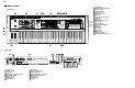
CS6X PANEL LAYOUT Front panel 1 GAIN MIC/LINE 2 6 LINE 1 A / D INPUT L/MONO PHONES VOLUME R OUTPUT 7 1 2 FOOT FOOT FOOT INDIVIDUAL OUTPUT VOLUME CONTROLLER SUSTAIN SWITCH FILTER IN BREATH TO HOST 9 10 OUT HOST SELECT 8 12 15 13 14 16 19 THRU 3.
CS6X CIRCUIT BOARD LAYOUT RIB DM PNA RV PNB PS LCD JK SM 5
CS6X BLOCK DIAGRAM 28CA1-8813234 6
CS6X WIRING 7
CS6X DISASSEMBLY PROCEDURE 1. Bottom Assembly Remove the thirty-five (35) screws marked [104], the two (2) corner plates, marked [102], and the two (2) coin screws marked [106]. The botton assembly can then be removed. SM, RV, Display Ass'y [104] 〈BOTTOM VIEW〉 Circuit Board & Unit Ref No. PARTS NAME PARTS No. Q'ty Fig. PLG Support Brecket 112 Bind Head Tapping Screw-B 3.0 X 6 MFZN2BL EP600230 5 2 SM 62 Bind Head Tapping Screw-B 3.
CS6X DM [122] [122] Fig.3 [32] [52] [42] RV PNB PNA LCD Assy SM [22] Fig.4 3. 3-1 3-2 Keyboard Assembly Remove the bottom assembly. (See Procedure 1.) Remove the four(4) screws marked [72]. The keyboard Assembly can then be removed.(Fig.
CS6X LSI PIN DESCRIPTION HD64F7045F28 (XW419A00) CPU PIN NAME I/O FUNCTION NO.
CS6X HD63B01Y0RCE0F (XM234A00) CPU (PKS) PIN NO. 1 2 3 4 5 6 7 8 9 10 11 12 13 14 15 16 17 18 19 20 21 22 23 24 25 26 27 28 29 30 31 32 NAME /NMI E D# D C# CL PULL 1 PULL 2 LC.
CS6X TC203C760HF-002 (XS725A00) SWP30B AWM Tone Generator coped with MEG) Standard Wave Processor 12 PIN NO.
CS6X MN101C027YB (XS711200) CPU PIN NO.
CS6X PCM1800 (XU770A00) A/D Converter PIN NAME I/O FUNCTION NO. 1 2 3 4 5 6 7 8 9 10 11 12 VINL VREF1 REFCOM VREF2 VINR RSTB BYPAS FMT0 FMT1 MODE0 MODE1 FSYNC I I I I I I I I I/O Analog input (L ch.) Reference 1 decoupling cap. Reference decoupling common Reference 2 decoupling cap. Analog input (R ch.) Reset input active “L” LCF bypass control Audio data format 0 Audio data format 1 Master/Slave mode selection 0 Master/Slave mode selection 1 Frame sync. input/output PIN NO.
CS6X 1 VCC 20 IN / OUT 2 19 G CLEAR 1 20 VCC A2 3 18 B1 1Q 2 19 8Q A3 4 17 B2 1D 3 18 8D A4 5 16 B3 2D 4 17 7D B4 2Q 5 16 7Q 6 2 GND 3 1CLR 1 1D 2 5 COUT CK D CL Q D CK CL Q 3Q B5 6 A7 8 13 B6 3D 7 A8 9 12 B7 4D 8 GND 10 11 B8 4Q 9 Q Q CL CK D CL D CK M5M34051FP(XV103A00) IC12 Line Transceiver 1 16 VCC 1A 2 15 1D 1R 3 14 1Y 1DE 4 13 1Z 2R 5 12 6D 13 5D 12 5Q 2DE 6 11 2Z 2A Inverting Input A 2B 7 10 2
CS6X CIRCUIT BOARDS DM Circuit Board CN19: to PNA-CN1 CN22: to SM-CN1 CN20: to JK-CN2 CN18: OPTION-MLAN-CN1 CN21: to JK-CN4 CN6: to RV-CN10 CN7: to PNA-CN3 CN15: to PLUG IN1-CN1 CN4: to JK-CN5 CN16: to PLUG IN2-CN1 CN13: CN12: to LCD-2P to LCD-CN1 CN14: to RV-CN11 CN17: to PNA-CN4 CN3: to LC-CN2 CN2: to LC-CN3 CN11: to PS-CN3 CN10: CN9: CN5: CN8: to KS-CN1 to RIB-CN14 to WHEEL-5P to JK-CN7 Component side Note : See parts list for details of circuit board component parts.
CS6X Pattern side Battery VN103500 VN103600(Battery holder for VN103500) • Notice for back-up battery removal Push the battery as shows in figure, then the battery will pop up. • Druk de batterij naar beneden zoals aangeven in de tekening, de batterij springt dan naar voren.
CS6X RIB Circuit Board RV Circuit Board CN15: from RIBBON CN9: to PNA-CN8 CN10: to DM-CN6 CN11: to DM-CN14 CN14: to DM-CN9 CN14: to DM-CN9 Component side Component side PNA Circuit Board CN1: CN2: to DM-CN19 to JK-CN1 CN3: to DM-CN7 CN5: to PNB-CN12 CN6: to PNB-CN13 CN4: to DM-CN17 CN7: CN8: to JK-CN6 to RV-CN9 Component side 18 RIB, RV, PNA: 2NA-V357940 1
CS6X PNB Circuit Board CN12: to PNA-CN5 CN13: to PNA-CN6 Component side SM Circuit Board CN1: to DM-CN22 PNB: 2NA-V357980 SM: 2NA-V357710 1 1 Component side Pattern side 19
CS6X JK Circuit Board ( B virsion) HOST SELECT PC2 PC1 MIDI THRU OUT IN MIDI to HOST BREATH FOOT SWITCH SUSTAIN FOOT FOOT CONTROLLER VOLUME INDIVIDUAL OUTPUT 2 Mac 1 OUTPUT R L/MONO PHONES A/D INPUT MIC/LINE2 LINE1 GAIN CN4: to DM-CN21 CN5: to DM-CN4 CN6: to PNA-CN7 JK Circuit Board ( C virsion) HOST SELECT PC2 PC1 MIDI THRU OUT CN7: to DM-CN8 IN MIDI to HOST BREATH FOOT SWITCH SUSTAIN CN2: to DM-CN20 FOOT FOOT CONTROLLER VOLUME CN1: to PNA-CN2 CN3: to PS-CN2 INDIVIDUAL
CS6X TEST PROGRAM Test No. Test Conditions, Judgment Criteria, etc. Test Item T1 RAM READ/WRITE OK/NG, (MAIN SRAM/WAVE DRAM) T2 RAM BATTERY OK/NG, 2.7V or more, Less than 3.
CS6X A. HOW TO ENTER THE TEST PROGRAM C. TEST SELECTION WHEN AN ERROR HAS BEEN DETECTED While pressing the [VOICE], [PERFORM] and [STORE] switches, turn on the [POWER ON/OFF] switch. The following message will then appear. When the test result has been judged as “NG” in each of the following tests, choose whether to execute the same test or to proceed to the next test. In this state, pressing the [EXIT] switch will cancel the test mode and restore the normal state.
CS6X DISPLAY OF RESULTS OK If the wrong switch is pressed, “NG” will appear and no sine wave will be output. If the correct switch is pressed after that, testing will proceed to the next switch. If the test results for all switches are satisfactory, “OK” will appear. The switches are checked in the following order. [VOICE]>[PERFORM]>[STORE]>[UTILITY]>[CARD]> [SEQ]>[EDIT]>[JOB]>[PLAY/STP]>[SHIFT]>[EF.BYPS]> [MASTER]>[EXIT].[ENTER]>[DEC/NO]>[INC/YES]> [PRE1]>[PRE2]>[INT]>[EXT]>[PLG1]>[PLG2]>[Q.
CS6X T7. KEYBOARD DISPLAY OF RESULTS OK This test is used to check that the keyboard functions properly by scaling 88 keys from A1 to C7. NG (The above shows the C1 check.) x x x x: velocity value of the key being pressed When the key on the LCD display works at a velocity of 0X10 to 0X6F, it is considered normal and that keys note is output. The test will then proceed to the next key test. If a wrong key is played, “NG” will appear and that note’s sound will not be output.
CS6X x x x: current knob value y y y: next target value ZZZ: name of the Knob being checked Checking order: [ATK][DCY][SUS][REL][POR][PCH] [SCN][PAN][ARP][TMP] DISPLAY OF RESULTS OK NG (No change in the message on the display) TEST END The test ends after the results have been displayed. When the test result is “NG”, refer to “C. TEST SELECTION WHEN AN ERROR HAS BEEN DETECTED”.
CS6X T14. BREATH CONTROLLER x x x: current value of the breath controller Operate the breath controller in the following order: Not blowing (122-127) - Blowing (0-5) - Not blowing (122-127) - Not blowing - Blowing - Not blowing, remove the jack when “EXTRACT PLUG!” appears on the LCD. At this time, check that the plug is not plugged in, the numbers change sequentially and that “OK” appears on the LCD. (The test is “OK” when the value is 34 or less.
CS6X DISPLAY OF RESULTS OK NG (No change in the message on the display) TEST END When the test results of all switches are satisfactory, “OK” will appear on the LCD and the testing will end. When the test result is “NG”, refer to “C. TEST SELECTION WHEN AN ERROR HAS BEEN DETECTED”. Set the master volume to Max and check that the following signals are output from OUTPUT-L, INDIV1 and 2, and PHONES (L). OUTPUT-L: 1 kHz ±1.5 Hz, sine wave, +6.
CS6X T21. A-D LEVEL, JACK Set the A/D GAIN volume to the maximum level. Input a 1 kHz sine wave of the following level through the A/D input port according to the instructions on the LCD. MIC: -40 dBm ±0 dBm LINE: -6 dBm ±0 dBm When a plug is connected to the jack, both “EXTRACT PLUG” appears and the A/D level appear. When a plug is not connected and the level is 2 or lower, “INSERT PLUG” appears and when a plug is inserted, the A/D level will be indicated.
CS6X NO-BOARD: board is not loaded. CONTROL: CONTROL line failure TEST END When the [EXIT] switch is pressed, the sound output will stop and the next test number will be set. T25. DISPLAY OF RESULTS When the factory settings are restored OK When the factory settings are not restored NG mLAN TEST END The test ends after the result is displayed. Connect the mLAN board to the mLAN slot and execute testing.
CS6X T28. EXIT (3) Turn on the power while pressing [EXIT] and [ENTER], and the system program will be loaded from SMART MEDIA and the operating power will be restored. (4) Turn on the power while pressing [DEC] and [INC], and the wave data will be loaded from SMART MEDIA, and the operating power will be restored. When testing is executed, the following message will appear on the LCD. When [YES] is pressed, testing will end.
CS6X 31
CS6X 32
CS6X 33
CS6X 34
CS6X 35
CS6X 36
CS6X 37
CS6X 38
CS6X 39
CS6X MIDI DATA FORMAT Many MIDI messages listed in the MIDI Data Format section are expressed in hexadecimal or binary numbers. Hexadecimal numbers may include the letter “H” as a suffix. The letter “n” indicates a certain whole number. The chart below lists the corresponding decimal number for each hexadecimal/binary number.
CS6X 2) RECEIVE FLOW 3) TRANSMIT/RECEIVE DATA MIDI > -[SW11]+--- NOTE OFF 8nH | | | +--- NOTE ON/OFF 9nH | | | +--- CONTROL CHANGE | | MODULATION BnH,01H | | PORTAMENTO TIME BnH,05H | | DATA ENTRY MSB BnH,06 | | DATA ENTRY LSB BnH,26H | | MAIN VOLUME BnH,07H | | PAN BnH,0AH | | EXPRESSION BnH,0BH | | SUSTAIN SWITCH BnH,40H | | PORTAMENTO SWITCH BnH,41H | | SOSTENUTO BnH,42H | | HARMONIC CONTENT BnH,47H | | EG RELEASE TIME BnH,48H | | EG ATTACK TIME BnH,49H | | BRIGHTNESS BnH,4AH | | EG DECAY TIME BnH,4BH
CS6X ank Select will be actually executed when the Program Change message is received. ank Select and Program Change numbers that are not supported by Yamaha will be gnored. (3-6-1-2)IDENTITY REQUEST(Receive only) F0H 7EH 0nH 06H 01H F7H ("n" = Device No.However, this instrument receives under "omni.
CS6X SEQ HOST MODE = MIDI KBD To Host From Host Local Sw MIDI Out MIDI In TG SEQ KBD HOST MODE = PC1/PC2/MAC To Host From Host Local Sw MIDI Out MIDI In TG Although three types of note on/note off data, received via MIDI, played by the internal sequencer and played on the keyboard will be distinguished, the other controllers (channel messages) equally affect the entire notes. ALL SOUNDS OFF clears all the sounds in the specific channel(s) played by both the keyboard and the data via MIDI.
CS6X 44
CS6X 45
PARTS LIST CONTENTS OVERALL ASSEMBLY .............................................. 2 PANEL ASSEMBLY ......................................... 4 WHEEL ASSEMBLY .................................... 5 MK ASSEMBLY .................................................... 6 POWER SUPPLY ASSEMBLY ............................ 7 ELECTRICAL PARTS .............................................
CS6X OVERALL ASSEMBLY 20 322 28 10 22 Panel Assembly (See page 4) 29 92 50 24 310 26 60 320 Wheel Assembly (See page 5) 450 62 400 92 510 40 110 130 42 94 120 110b 110a 92 90 500 490 Power Supply Assembly (See page 7) 112 430 92 30 300 MK Assembly (See page 6) 32 70 304 440 122 305 302 480 470 100a 74 460 74 420 100d 100b 100c 410 106 72 104 100 102 104 2
CS6X REF NO. * * * * * * * * * * * 10 20 22 24 26 28 29 30 32 40 42 50 60 62 70 72 74 76 90 90 92 100 100a 100b 100c 100d 102 104 106 110 110a 110b 112 120 122 125 126 127 128 130 300 302 304 305 310 312 314 320 322 324 326 400 410 420 430 440 450 460 470 490 500 PART NO.
CS6X PANEL ASSEMBLY REF NO. PART NO. DESCRIPTION PANEL ASSEMBLY Panel Assembly Control Panel Cover (S) Flat Head Screw Display Assembly Bind Head Tapping Screw-B Circuit Board Assembly Circuit Board Push Button REMARKS * * --V3272300 VS863000 -EP600230 -V3579500 V4162700 * 30c V 4 1 6 2 6 0 0 Push Button * * 32 34 36 40 40a 40b EP600230 CB069250 CB829850 -V3579800 V3887400 * 40c V 4 1 6 2 7 0 0 Push Button 3.
CS6X WHEEL ASSEMBLY 70 10 60 90 80 80 90 50 10 40 40 20 30 40 20 REF NO. * 10 20 20 30 40 50 60 70 80 90 PART NO. -VF536800 VQ546400 V4579900 VC792800 CB819020 EW600110 VQ764300 VN245400 -CB069250 : New Parts DESCRIPTION WHEEL ASSEMBLY Wheel Assembly Frame Wheel Wheel Spring Wheel Tube Stop Ring Rotary Variable Resistor Rotary Variable Resistor Connector Assembly Cord Holder REMARKS QTY RANK 2 2 2 02 06 CS6X (V387160) Since 1999,11,01 2 12.0 RK1631110T54A 10K 10.
CS6X MK ASSEMBLY 1 1f 10 1c 1d 1e 1b 1d 3 1a 4 6 2 5 20 22 10 20 22 DESCRIPTION MK ASSEMBLY MK Assembly -VN399200 Keyboard Assembly Front Rail -EP600230 Bind Head Tapping Screw-B 1 1a 1b 1b 1b 1b 1b 1b 1c 1d 1e 1f 2 3 4 5 6 VN399200 VN405500 -VL570000 VL570100 VL570200 VL570300 VL570400 VL570500 VL570600 VC077600 VR857100 VN406100 VI912000 VF834100 VM630100 EP630630 VC079800 REF NO. PART NO.
CS6X POWER SUPPLY ASSEMBLY REF NO. * * 10 20 20 30 40 40a 42 50 50a 52 54 56 PART NO.
CS6X ELECTRICAL PARTS REF NO. * * * * * * * * * * * * BT1 CN1 CN2 CN3 CN4 CN5 CN6 CN7 CN8 CN9 CN10 CN12 CN13 CN14 CN15 CN16 CN17 CN18 CN19 CN20 CN21 CN22 D1 -7 D10 -15 D17 -19 D20 D22 -24 D41 D42 D49 -51 D52 -55 D57 -60 D61 D62 D65 D66 D68 -71 D73 EM1 -13 EM15 -17 IC1 IC2 IC3 IC4 IC5 IC6 IC7 IC8 IC9 PART NO.
CS6X REF NO. * * * * IC10 IC11 IC12 IC13 -16 IC17 IC18 IC19 IC20 IC21 IC22 IC23 IC26 IC27 IC28 IC29 IC30 IC31 IC32 IC34 IC36 IC37 IC38 IC42 IC43 IC45 IC47 IC48 IC50 IC51 IC52 IC54 IC55 IC56 IC60 IC61 IC62 IC63 IC64 IC65 IC66 IC68 IC71 IC72 IC73 IC74 IC75 IC100 IC101 IC102 IC103 L2 L3 -20 L23 -48 L52 -67 L70 L102 L103 L106 -112 L114 RA1 -15 RA16 -27 RA28 RA29 PART NO.
CS6X REF NO. RA30 RA31 -33 RA34 RA35 RA36 RA37 RA38 RA39 RA40 RA41 RA42 RA43 RA44 -48 RA50 RA51 RA60 -74 RA82 RA83 RA85 RA86 TR1 TR2 TR3 TR4 TR5 TR6 TR7 -10 TR11 TR12 X1 X2 X3 ZD1 PART NO.
CS6X REF NO. PART NO. DESCRIPTION UF037470 Electrolytic Cap. (chip) * UF038100 UF046470 UF066100 UF066330 UF138220 UF147470 UF148220 UR629220 VP473600 Electrolytic Cap. (chip) Electrolytic Cap. (chip) Electrolytic Cap. (chip) Electrolytic Cap. (chip) Electrolytic Cap. (chip) Electrolytic Cap. (chip) Electrolytic Cap. (chip) Electrolytic Capacitor Electrolytic Capacitor 100 16V 4.7 25V 1 50V 3.3 50V 220 16V UUR1C2 47 25V UUR1E4 220 25V UUR1E2 2200 10.0V 100.00 10.
CS6X REF NO. 20 30 40 50 60 C62 CN1 CN2 CN3 CN4 CN5 CN6 CN7 D1 -4 EM1 -3 IC1 IC2 -4 J J1 J2 -5 J7 -11 J12 J13 J16 J19 J20 J21 J22 J23 JK1 JK2 -5 JK6 JK7 JK8 JK9 JK10 JK11 JK12 JK13 JK14 L1 -22 L24 -32 L33 R84 SW1 TR2 TR4 -9 VR1 WJ1 PART NO.
CS6X REF NO. PART NO. DESCRIPTION HF454560 Carbon Resistor HF455100 Carbon Resistor 56.0 1/4 J 100.0 1/4 J HF455220 Carbon Resistor HF455470 Carbon Resistor HF456100 Carbon Resistor 220.0 1/4 J 470.0 1/4 J 1.0K 1/4 J Carbon Resistor Carbon Resistor Carbon Resistor Carbon Resistor 1.8K 1/4 J 2.7K 1/4 J 4.7K 1/4 J 10.0K 1/4 J HF457120 Carbon Resistor HF457220 Carbon Resistor HF457470 Carbon Resistor 12.0K 1/4 J 22.0K 1/4 J 47.
CS6X J3 J4 J6 -9 LD1 -13 PART NO. VA078900 VA078900 VA078900 VA078900 VS704700 VS704700 RA1 SW1 -19 V F 7 7 1 9 0 0 Resistor Array VZ085500 Tact Switch VZ085500 Tact Switch RGLE8X103J SKQNAM004A SKQNAM004A VR1 VR2 -20 V 3 6 2 5 5 0 0 Rotary Variable Resistor V 4 1 0 2 9 0 0 Rotary Variable Resistor V 4 1 0 2 9 0 0 Rotary Variable Resistor A10.0K RK14K124 B 10.0K RK11K114 B 10.0K RK11K114 REF NO. * * * * * * D20 -55 J J5 LD14 LD15 SW20 -55 * * CN1 CN2 REMARKS 0.55 0.55 0.55 0.
A B C D E F G H I J K L M N O P Q CS6X CIRCUIT DIAGRAM 1/4 (DM1/3) 1 CS6X 1 2200/10 to SV-CN3 to JK-CN5 to PS-CN3 INVERTER to JK-CN7 to RV-CN5 2 2 to WHEEL PHOTOCOUPLER to RIBBON LINE TRANSCEIVER KEYBOARD CN1,CN3 OP AMP 3 3 CPU 4 4 INVERTER MPX MPX to DM2/3 B8 KEYBOARD CN2,CN4 MPX to LC KEYBOARD MPX INVERTER to DM3/3 B6 5 C200 D-FF INVERTER D-FF INVERTER 5 to RV-CN6 220/10 6 to DM2/3 D10 to DM2/3 P4 6 to DM3/3 B6 to DM3/3 B6 100P 100P 100P 100
A B C D E F G H I J K L M N O P Q 1 1 2 2 3 3 4 4 5 5 6 6 7 7 8 8 9 9 10 10 11 11 12 12 A B C D E F G H I J K L M N O P Q
A B C D E F G H I J K L M N O P Q 1 1 2 2 3 3 4 4 5 5 6 6 7 7 8 8 9 9 10 10 11 11 12 12 A B C D E F G H I J K L M N O P Q
1 2 3 4 5 6 7 8 9 10 11 12 CS6X CIRCUIT DIAGRAM 4/4 (PNA, PNB, JK, RIB) A CS6X PNA A PNB B B C C RIB to JK-CN6 D D to RIBBON to DM -CN17 to DM-CN9 to DM -CN19 E E to JK -CN1 F F SM RV G G to DM-CN22 H H 28CC1-8813231 1 I I R90 100 JK 100 OPAMP J J PHONES 47K 100 OPAMP OPAMP 0.01 R91 1M 100 GAIN to DMCN21 to DM-CN4 100 OPAMP J25 L8 J24 K J6 0.01 K OPAMP 0.1 to SV -CN2 OPAMP 0.1 0.1 SUSTAIN L 0.01u Foot Switch L 0.