YMF724F Preliminary DS-1 OVERVIEW YMF724F (DS-1) is a high performance audio controller for the PCI Bus. DS-1 consists of two separated functional blocks. One is the PCI Audio block and the other is the Legacy Audio block. PCI Audio block allows Software Driver to handle maximum of 73 concurrent audio streams with the Bus Master DMA engine. The PCI Audio Engine converts the sampling rate of each audio stream and the streams are mixed without utilizing the CPU or causing system latency.
YMF724F LOGOS GENERAL MIDI logo is a trademark of Association of Musical Electronics Industry (AMEI), and indicates GM system level 1 Compliant. XG logo is a trademark of YAMAHA Corporation. SONDIUS-XG logo is a trademark that Stanford University in the United States and YAMAHA Corporation hold jointly. Sensaura logo is a trademark of Central Research Laboratories Limited. 1.
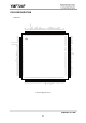
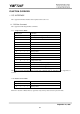
YMF724F PIN CONFIGURATION 144 143 142 141 140 139 138 137 136 135 134 133 132 131 130 129 128 127 126 125 124 123 122 121 120 119 118 117 116 115 114 113 112 111 110 109 GREF GP3 GP2 GP1 GP0 ROMDI/TEST2# TEST1# TEST0# NC LVSS LOOPF1 LOOPF0 LVDD ROMCS TEST4# VDD5 XO24 XI24 VSS VSS VDD3 DIT TEST7# TEST6# TEST5# CMCLK CSDO CBCLK CSDI CSYNC CRST# TEST3# NC NC NC ASDI YMF724F-V 1 2 3 4 5 6 7 8 9 10 11 12 13 14 15 16 17 18 19 20 21 22 23 24 25 26 27 28 29 30 31 32 33 34 35 36 XRST# ACS# ACDO ACDI ASCLK ASDO
YMF724F PIN DESCRIPTION 1.
YMF724F 3.
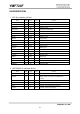
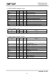
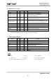
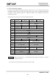
YMF724F 6. Miscellaneous (15-pin) name I/O type Size ROMCS O T 3mA ROMSK / VOLUP# IO Tup 3mA ROMDO / VOLDW# IO Tup 3mA ROMDI / TEST2# I Tup - XI24 I C - 24.576 MHz Crystal XO24 O C 2mA 24.
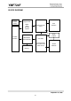
YMF724F BLOCK DIAGRAM PC-PCI / D-DMA / S-IRQ Legacy Audio SBPro OPL3 MPU401 Joystick Rate Converter / Mixer AC-2 Interface SPDIF (output) PCI Bus Interface BUS Master DMA Controller PCI Audio XG Synthesizer Direct Sound Acc.
-8- Joystick Vjoyd.vxd Msjstck.
YMF724F FUNCTION OVERVIEW 1. PCI INTERFACE DS-1 supports the PCI bus interface and complies to PCI revision 2.1. 1-1. PCI Bus Command DS-1 supports the following PCI Bus commands. 1-1-1.
YMF724F 1-2. PCI Configuration Register In addition to the Configuration Register defined by PCI Revision 2.1, DS-1 provides proprietary PCI Configuration Registers in order to control legacy audio function, such as OPL3, Sound Blaster Pro, MPU401 and Joystick. These additional registers are configured by BIOS or the configuration software from YAMAHA Corporation. The following shows the overview of the PCI Configuration Register. Offset b[31..24] b[23..16] b[15..8] b[7..
YMF724F 00 - 01h: Vendor ID Read Only Default: 1073h Access Bus Width: 8, 16, 32-bit b15 b14 b13 b12 b11 b10 b9 b8 b7 b6 b5 b4 b3 b2 b1 b0 Vendor ID b[15:0] ........Vendor ID This register contains the YAMAHA Vendor ID registered in Revision 2.1. This register is hardwired to 1073h. 02 - 03h: Device ID Read Only Default: 000Dh Access Bus Width: 8, 16, 32-bit b15 b14 b13 b12 b11 b10 b9 b8 b7 b6 b5 b4 b3 b2 b1 b0 Device ID b[15:0] ........
YMF724F b8................SER: SERR# Enable This bit enables DS-1 to drive SERR#. “0”: Do not drive SERR#. (default) “1”: Drives SERR# when DS-1 detects an Address Parity Error on normal target cycle or a Data Parity Error on special cycle. 06 - 07h: Status Read / Write Clear Default: 0210h Access Bus Width: 8, 16, 32-bit b15 b14 b13 b12 b11 DPE SSE RMA RTA STA b10 b9 DEVT b4................
YMF724F 08h: Revision ID Read Only Default: 03h Access Bus Width: 8, 16, 32-bit b7 b6 b5 b4 b3 b2 b1 b0 Revision ID b[7:0] ..........Revision ID This register contains the revision number of DS-1. This register is hardwired to 03h. 09h: Programming Interface Read Only Default: 00h Access Bus Width: 8, 16, 32-bit b7 b6 b5 b4 b3 b2 b1 b0 Programming Interface b[7:0] ..........Programming Interface This register indicates the programming interface of DS-1.
YMF724F 0Dh: Latency Timer Read / Write Default: 00h Access Bus Width: 8, 16, 32-bit b7 b6 b5 b4 b3 b2 b1 b0 Latency Timer b[7:0] ..........Latency Timer When DS-1 becomes a Bus Master device, this register indicates the initial value of the Master Latency Timer. 0Eh: Header Type Read Only Default: 00h Access Bus Width: 8, 16, 32-bit b7 b6 b5 b4 b3 b2 b1 b0 Header Type b[7:0] ..........Header Type This register indicates the device type of DS-1. This is hardwired to 00h.
YMF724F 2C-2Dh: Subsystem Vendor ID Read Only Default: 1073h Access Bus Width: 8, 16, 32-bit b15 b14 b13 b12 b11 b10 b9 b8 b7 b6 b5 b4 b3 b2 b1 b0 Subsystem Vendor ID b[15:0] ........Subsystem Vendor ID This register contains the Subsystem Vendor ID. In general, this ID is used to distinguish adapters or systems made by different IHVs using the same chip by the same vendor. This register is read only. To write the IHV’s Vendor ID, use 44-45h (Subsystem Vendor ID Write Register).
YMF724F 3Ch: Interrupt Line Read / Write Default: 00h Access Bus Width: 8, 16, 32-bit b7 b6 b5 b4 b3 b2 b1 b0 Interrupt Line b[7:0] ..........Interrupt Line This register indicates the interrupt channel that INTA# is assigned to. 3Dh: Interrupt Pin Read Only Default: 01h Access Bus Width: 8, 16, 32-bit b7 b6 b5 b4 b3 b2 b1 b0 Interrupt Pin b[7:0] ..........Interrupt Pin DS-1 supports INTA# only. This register is hardwired to 01h.
YMF724F 40 - 41h: Legacy Audio Control Read / Write Default: 907Fh Access Bus Width: 8, 16, 32-bit b15 b14 LAD SIEN b13 b12 b11 b10 MPUIRQ b9 b8 b7 SBIRQ b6 SDMA b5 b4 b3 I/O MIEN b2 b1 MEN GPEN FMEN SBEN b0................SBEN: Sound Blaster Enable This bit enables the mapping of the Sound Blaster Pro block in the I/O space specified by the SBIO bits, when LAD is set to “0”.
YMF724F b[7:6] ..........SDMA: Sound Blaster DMA-8 Channel Select These bits select the DMA channel for the Sound Blaster Pro block. “0”: DMA ch0 “1”: DMA ch1 “2”: reserved “3”: DMA ch3 (default) b[10:8] ........SBIRQ: Sound Blaster IRQ Channel Select These bits select the interrupt channel for the Sound Blaster Pro block. “0”: IRQ5 “1”: IRQ7 “2”: IRQ9 “3”: IRQ10 “4”: IRQ11 “5” - “7”: reserved. (default) b[13:11] ......
YMF724F 42 - 43h: Extended Legacy Audio Control Read / Write Default: 0000h Access Bus Width: 8, 16, 32-bit b15 IMOD b14 b13 SBVER b12 b11 SMOD b10 b9 b8 - - MAIM b7 b6 JSIO b5 b4 b3 MPUIO b2 SBIO b1 b[1:0] ..........FMIO: FM I/O Address allocation These bits determine the base I/O address for the of the OPL3 block (FMBase). OPL3 block uses 4 bytes in the I/O address space. “0”: 388h “1”: 398h “2”: 3A0h “3”: 3A8h (default) b[3:2] ..........
YMF724F b[12:11] ......SMOD: SB DMA mode These bits determine the protocol to achieve the DMAC(8237) function on the PCI bus. “0”: PC/PCI (default) “1”: reserved “2”: Distributed DMA “3” reserved b[14:13] ......SBVER: SB Version Select These bits set the version of the SB Pro DSP. The value set in these bits is returned by sending the E1h DSP command. “0”: ver 3.01 “1”: ver 2.01 “2”: ver 1.05 “3”: reserved (default) b15..............
YMF724F 46-47h: Subsystem ID Write Register Read / Write Default: 000Dh Access Bus Width: 16-bit b15 b14 b13 b12 b11 b10 b9 b8 b7 b6 b5 b4 b3 b2 b1 b0 Subsystem ID Write b[15:0] ........Subsystem ID Write Register This register sets the Subsystem ID that is read from 2E-2Fh (Subsystem ID register). The default value is the DS-1 Device ID, 000Dh. IHVs must change this ID to their ID in the BIOS POST routine.
YMF724F b2................DPLL1: Disable PLL1 Clock Oscillation Setting this bit to “1” disables the oscillation of PLL for the PCI Audio function. “0”: Normal (default) “1”: Disable b3................PSL0: Power Save Legacy Audio Block 0 Setting this bit to “1” stops providing the clock with the Legacy Audio function block 0. This block includes OPL3 and SB Pro engines. “0”: Normal (default) “1”: Power Save b4................
YMF724F b12..............PR4: AC-2 Power down Control 4 This bit controls the power state of the AC-link in AC-2. “0”: Normal (default) “1”: Power down b13..............PR5: AC-2 Power down Control 5 Setting this bit to “1” disables the internal clock of AC-2. clock is supplied from DS-1. In case AC-2 is used with DS-1, the master Therefore, when the clock of AC-2 is stopped completely, set both PR5 and PSN bits to “1”. “0”: Normal (default) “1”: Disable b[15:14] ......
YMF724F 4C-4Dh: D-DMA Slave Configuration Read / Write Default: 0000h Access Bus Width: 8, 16, 32-bit b15 b14 b13 b12 b11 b10 b9 b8 b7 b6 b5 Base Address b4 b3 EA b2 b1 TS b0................CE: Channel Enable This bit enables the Distributed DMA function. “0”: Disable Distributed DMA (default) “1”: Enable Distributed DMA b[2:1] ..........TS: Transfer Size These bits indicate the size of the DMA transfer. Since DS-1 supports only 8-bit DMA transfer, the bits are hardwired to 00b. b3........
YMF724F 51h: Next Item Pointer Read Only Default: 00h Access Bus Width: 8, 16, 32-bit b7 b6 b5 b4 b3 b2 b1 b0 Next Item Pointer b[7:0] ..........Next Item Pointer DS-1 does not provide other new capability besides Power Management. This register is hardwired to 00h. 52-53h: Power Management Capabilities Read Only Default: 0401h Access Bus Width: 8, 16, 32-bit b15 b14 b13 b12 b11 b10 b9 b8 b7 b6 b5 b4 b3 - - - - - D2S D1S - - - - - - b2 b1 Version b[2:0] ..........
YMF724F 54-55h: Power Management Control / Status Read / Write Default: 0000h Access Bus Width: 8, 16, 32-bit b15 b14 b13 b12 b11 b10 b9 b8 b7 b6 b5 b4 b3 b2 - - - - - - - - - - - - - - b1 b0 PS b[1:0] ..........PS: Power State These bits determine the power state of DS-1. “0”: D0 “1”: D1 “2”: D2 “3”: D3hot DS-1 supports the following power states: (not supported) When the power state is changed from D3hot to D0, DS-1 resets the PCI Configuration register 00-3Fh.
YMF724F 2. ISA Compatible Device DS-1 contains the following functions to maintain the compatibility with the past ISA Sound Devices. These devices are considered Legacy devices and the functions are referred to as Legacy Audio. Legacy Audio is independent from PCI Audio and can be used simultaneously. The configuration is set in the Legacy Audio Control Register in the PCI Configuration Register space. Basically, these registers are configured by the BIOS.
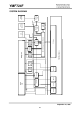
YMF724F DS-1 supports PC/PCI and D-DMA protocols to emulate the DMA of SB Pro on the PCI. In addition, DS-1 supports the old type of interrupts used by ISA and the Serialized IRQ protocol. Yamaha recommends the combination of PC/PCI and Serialized IRQ. The system block diagram when using Intel 430TX chip set is shown below.
YMF724F 2-1. OPL3 Block OPL3 Block is register compatible with YMF289B. However, Power Management register has been deleted because it is now controlled by the PCI Configuration Register. The following shows the FMBase I/O map of OPL3. FMBase (R) Status Register port FMBase (W) Address port for Register Array 0 FMBase+1 (R/W) Data port FMBase+2 (W) Address port for Register Array 1 FMBase+3 (R/W) Data port The default FMBase value is 0x0388. The following shows the OPL3 Block registers.
YMF724F 2-1-2.
YMF724F 2-2. Sound Blaster Pro Block This block emulates the DSP commands of Sound Blaster and Sound Blaster Pro. functions are supported (record functions are not supported). Only playback However, to maintain compatibility for games, it is designed so that every DSP command receives a correct response. The DMA transfer of this block uses PC/PCI or D-DMA protocol. The following shows the SBBase I/O map of SB Pro.
YMF724F 2-2-1. DSP Command The following shows the list of DSP Commands that are supported by the SB Pro engine. Both SB and SB Pro commands are supported.
YMF724F 2-2-2. Sound Blaster Pro Mixer The following shows the register map of the Mixer section of Sound Blaster Pro. Address b7 b6 b5 b4 00h b3 b2 b1 b0 04h Voice Volume L "1" 0Ah - - 0Ch - - Ifilter* "1" 0Eh - - Ofilter* "1" - Voice Volume R "1" - "1" MIC Volume* Input Source* "1" - "1" - St.
YMF724F (1) Volume for MIDI MIDI Vol. (26h) 0 Master Vol.
YMF724F 2-2-3. SB Suspend / Resume The SB block can read the internal state as to support Suspend and Resume functions. is made up of 218 flip flops. The internal state To read the state, these states are shifted in order and read 8 bits at a time from the SCAN DATA register. These registers are mapped to the SB Mixer space (see SB Mixer Register map). The registers have the following functions.
YMF724F F1h: Scan In/ Out Data Read / Write Default: 00h b7 b6 b5 b4 b3 b2 b1 b0 SCAN DATA b[7:0] ..........SCAN DATA This is the data port for reading and writing the internal state. F8h: Interrupt Flag Register Read Only Default: 00h b7 b6 b5 b4 b3 b2 b1 b0 - - - - - - - SBI b0................SBI: SB Interrupt Flag This bit indicates that the SB DSP occurs the interrupt. read port to clearing the interrupt and this bit. This bit is read only.
YMF724F 2-3. MPU401 This block is for transmitting and receiving MIDI data. It is compatible with UART mode of “MPU401”. Full duplex operation is possible using the 16-byte FIFO for each direction, transmitting and receiving. The following shows the MPUBase I/O map for MPU401. MPUBase (R/W) MIDI Data port MPUBase + 1h (R) Status Register port MPUBase + 1h (W) Command Register port port D7 D6 D5 D4 D3 +0h Data +1h (W) Command +1h (R) /DSR D2 D1 D0 /DRR - - - - - - 2-4.
YMF724F 3. DMA Emulation Protocol The former synthesizer LSI for the ISA bus such as the Sound Blaster used the DMA controller (8237: ISA DMAC) on the system to transfer the sound data from/to the host. For DS-1, however, ISA DMAC must be used to transfer the sound data to the Sound Blaster Pro Block of the Legacy Audio Block. Because signals to connect to the ISA DMAC are generally not available on the PCI bus, there are two ways proposed from the industry to emulate the ISA DMAC on the PCI bus.
YMF724F 3-2. D-DMA DS-1 provides the following registers to support D-DMA. D-DMA Slave Configuration Register (4C-4Dh) of the PCI Configuration register is used to set the Base address of the Slave Address.
YMF724F 4. Interrupt Routing DS-1 supports three types of interrupts, interrupt signal on the PCI bus (INTA#), interrupt signal on the ISA bus (IRQ[5,7,9,10,11]), and Serialized IRQ. The IRQs on DS-1 are routed as shown below.
YMF724F 6. Hardware Volume Control The hardware volume control determines the AC-2 master volume without using any software control using the external circuit listed below. Two pins, VOLUP# for increasing the volume and VOLDW# for decreasing the volume, are used. Push SW 1k VOLUP# Push SW 1k VOLDW# 1000p 1000p DS-1 provides a shadow register for the AC-2 master volume. When the software accesses the AC-2 Master Volume, it is always reflected in the shadow register.
YMF724F ELECTRICAL CHARACTERISTICS 1. Absolute Maximum Ratings Item Symbol Min. Max. Unit Power Supply Voltage 1 (PVDD, VDD5) VDD5 -0.5 7.0 V Power Supply Voltage 2 (VDD3, LVDD) VDD3 -0.3 4.6 V Input Voltage 1 (PVDD, VDD5) VIN5 -0.5 VDD5+0.5 V Input Voltage 2 (VDD3, LVDD) VIN3 -0.3 VDD3+0.3 V Operating Ambient Temperature TOP 0 70 °C Storage Temperature TSTG -50 125 °C Note : PVSS=LVSS=VSS=0[V] 2. Recommended Operating Conditions Item Symbol Min. Typ. Max.
YMF724F 3. DC Characteristics Item Symbol Condition Min. Typ. Max. Unit High Level Input Voltage 1 VIH1 *1 2.2 VDD5 +0.5 V Low Level Input Voltage 1 VIL1 *1 -0.5 0.8 V High Level Input Voltage 2 VIH2 *2 2.2 VDD5 +0.5 V Low Level Input Voltage 2 VIL2 *2 -0.5 0.6 V High Level Input Voltage 3 VIH3 *3 2.2 Low Level Input Voltage 3 VIL3 *3 High Level Input Voltage 4 VIH4 *4 Low Level Input Voltage 4 VIL4 *4 Input Leakage Current IIL V 0.8 0.
YMF724F 4. AC Characteristics 4-1. Master Clock (Fig.1) Item Symbol Min. Typ. Max. Unit XI24 Cycle Time tXICYC - 40.69 - ns XI24 High Time tXIHIGH 16 - 24 ns XI24 Low Time tXILOW 16 - 24 ns Note : Top = 0-70°C, PVDD=5.0±0.25 V, VDD5=5.0±0.25 V, VDD3=3.3±0.3 V, LVDD=3.3±0.3 V 3.5 V 2.5 V XI24 1.0 V t XIHIGH t XILOW t XICYC Fig.1: XI24 Master Clock timing 4-2. Reset (Fig.
YMF724F 4-3. PCI Interface (Fig.3, 4) Item Symbol Condition Min. Typ. Max.
YMF724F 4-4. AC-2 / AC3F2 Master Clock Item (Fig.5) Symbol Min. Typ. Max. Unit CMCLK Cycle Time tCMCYC - 40.69 - ns CMCLK High Time tCMHIGH 8 - - ns CMCLK Low Time tCMLOW 8 - ns CMCLK Rising Time tCMR - 4.6 - ns CMCLK Falling Time tCMF - 2.1 - ns Note : Top = 0-70°C, PVDD=5.0±0.25 V, VDD5=5.0±0.25 V, VDD3=3.3±0.3 V, LVDD=3.3±0.3 V, CL=50 pF t CMR t CMF 3.5 V 2.5 V CMCLK 1.0 V t CMHIGH t CMLOW t CMCYC Fig.5: Master Clock timing for AC-2 and AC3F2 4-5. AC-link (Fig.
YMF724F t CBICYC 2.0 V CBCLK 1.5 V t CBIHIGH 0.8 V t CBILOW t COH t CSYLOW t CVAL 2.0 V CSYNC 1.5 V 0.8 V t CSYHIGH t CSYCYC t CVAL t COH 2.0 V CSDO 0.8 V t CISU t CIH 2.0 V CSDI 0.8 V Fig.6: AC-link timing 4-6 AC3F2 Interface (Fig.7, 8) Item Symbol Condition Min. Typ. Max.
YMF724F t ASCCYC 2.0 V 1.5 V ASCLK 0.8 V t ASCHIGH t ASCLOW t ACVAL t ACOH 2.0 V ACS, ACDO 0.8 V t ACISU t ACIH 2.0 V ACDI 0.8 V Fig.7: AC3F2 Control Interface timing t ABICYC 2.0 V 1.5 V ABCLK 0.8 V t ABIHIGH t ABILOW t ASVAL t ASOH 2.0 V ASDO, ALRCK 0.8 V t ASISU t ASIH 2.0 V ASDI 0.8 V Fig.
YMF724F EXTERNAL DIMENSIONS YMF724F-V 22.00±0.40 20.00±0.30 73 72 144 37 1.40±0.20 1 1.70MAX. 0 MIN. (STAND OFF) 20.00±0.30 109 22.00±0.40 108 36 0.20±0.10 P-0.50TYP (1.00) 0-10˚ LEAD THICKNESS : 0.15+0.10 -0.06 0.50±0.20 The shape of the molded corner may slightly different from the shape in this diagram. The figure in the parenthesis ( ) should be used as a reference. Plastic body dimensions do not include burr of resin.
YMF724F IMPORTANT NOTICE 1. Yamaha reserves the right to make changes to its Products and to this document without notice. The information contained in this document has been carefully checked and is believed to be reliable. However, Yamaha assumes no responsibilities for inaccuracies and makes no commitment to update or to keep current the information contained in this document. 2.