YSP-1 SERVICE MANUAL IMPORTANT NOTICE This manual has been provided for the use of authorized YAMAHA Retailers and their service personnel. It has been assumed that basic service procedures inherent to the industry, and more specifically YAMAHA Products, are already known and understood by the users, and have therefore not been restated.
YSP-1 YSP-1 ■ TO SERVICE PERSONNEL WALL OUTLET 1. Critical Components Information Components having special characteristics are marked s and must be replaced with parts having specifications equal to those originally installed. 2. Leakage Current Measurement (For 120V Models Only) When service has been completed, it is imperative to verify that all exposed conductive surfaces are properly insulated from supply circuits. ● Meter impedance should be equivalent to 1500 ohms shunted by 0.15µF.
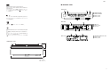
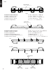
YSP-1 YSP-1 ■ FRONT PANEL J model only ■ REAR PANELS BOTTOM VIEW U, C models B, G models R model T model K model A model L model J model 3
YSP-1 YSP-1 ■ REMOTE CONTROL PANELS ■ SPECIFICATIONS / 参考仕様 U, C, R, T, K, A, B, G, L models ■ Audio Section / オーディオ部 Minimum RMS Output Power (Power Amp. Section) / 定格出力 (パ ワーアンプ部) Woofer [100Hz, 10%THD, 4 ohms] ................................. 20W x 2 Tweeter [1kHz, 10%THD, 10 ohms] ................................ 2W x 40 Input Jack / 入力端子 AUX, TV ................................................................ 1V / 32 k-ohms Output Jack / 出力端子 VIDEO ................................................
YSP-1 ■ INTERNAL VIEW Manufactured under license from Dolby Laboratories. “Dolby”, “Pro Logic”, and the double-D symbol are trademarks of Dolby Laboratories. FRONT VIEW ドルビーラボラトリーズからの実施権により製造されています。 「ドル ビー」、「PRO LOGIC」およびダブルD記号 は、ドルビーラボラト リーズの商標です。 1 2 2 1 1 DRIVER, WOOFER 2 DRIVER, TWEETER 3 INPUT (3) P.C.B. 4 INPUT (4) P.C.B. “DTS”, and “Neo:6” are trademarks of Digital Theater Systems, Inc.
SELECT MENU C) ROOM EQ B) BEAM ADJ A) PARAMETER E) TONE CONTROL D) AUDIO SET C) DYNAMIC RANGE B) SPEAKER LEVEL d) FOCAL LENGTH c) DISTANCE b) VERTICAL ANGLE a) HORIZ.
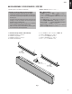
YSP-1 YSP-1 ■ DISASSEMBLY PROCEDURES / 分解手順 (番号順に部品を取り外してください。) (Remove parts in the order as numbered.) Cautions for disassembly and reassembly : 分解・組立時の注意: • Disconnect the power cable from the AC outlet. • Spread soft cloth or the like and perform the work on it. • Use full care as you may be injured by the front grille or other part. • All screws must be tightened securely to prevent air leakage. Check the number of screws and their positions when installing them.
YSP-1 YSP-1 3 3 3 3 3 3 3 3 Fig. 2 2. Removal of Rear Unit 2. リアユニットの外し方 a. Remove 22 screws (3). (Fig. 2) b. Remove CB7, CB10 and CB14. (Fig. 3) c. Remove the Rear Unit. a. ③のネジ 22本を外します。(Fig. 2) b. コネクター CB7、CB10、CB14を外します。(Fig. 3) c. リアユニットを取り外します。 Rear Unit リアユニット CB14 CB7 CB10 Fig. 3 When checking the P.C.B. : P.C.B.チェックをする場合には • The Rear Unit removed from the unit does not work because its grounding is loose.
YSP-1 YSP-1 Plate/ Shield プレート/シールド 4 Pad L パッドL 4 4 4 4 4 Fig. 4 3. Removal of INPUT (2) P.C.B. 3. INPUT(2)P.C.B.の外し方 a. b. c. d. e. f. a. b. c. d. e. f. Remove 14 screws (4). (Fig. 4) Remove 3 pad L’s. (Fig. 4) Remove the Plate/Shield. Remove 4 screws (5). (Fig. 5) Remove CB7, CB9 and CB302. (Fig. 5) Remove the INPUT (2) P.C.B.. CB302 CB9 CB7 ④のネジ 14本を外します。(Fig. 4) パッドL 3個を外します。(Fig. 4) プレート/シールドを取り外します。 ⑤のネジ 4本を外します。(Fig. 5) コネクター CB7、CB9、CB302を外します。(Fig. 5) INPUT(2)P.C.B.
YSP-1 YSP-1 Front Panel Unit フロントパネルユニット 8 8 8 8 8 Fig. 7 5. Removal of Front Panel Unit 5. フロントパネルユニットの外し方 a. b. c. d. a. b. c. d. Remove 17 screws (8). (Fig. 7) Remove the Front Panel Unit. Remove 2 screws (9). (Fig. 8) Remove the Stopper frame. ⑧のネジ 17本を外します。(Fig. 7) フロントパネルユニットを取り外します。 ⑨のネジ 2本を外します。(Fig. 8) ストッパーフレームを取り外します。 Stopper Frame ストッパーフレーム 9 Fig. 8 6. Removal of Driver (Tweeter) 6. スピーカーユニット(ツイーター)の外し方 a. b. c. d. e. a. b. c. d. e. Remove 12 screws (0). (Fig.
YSP-1 YSP-1 A Fig. 11 Installation of Driver (Tweeter) スピーカーユニット(ツイーター)の取り付け方 Caution : Make sure that all the removed Driver (tweeter) parts are reinstalled at specified positions. (Fig. B) 注意:取り外したスピーカーユニット (ツイーター)はすべ て決められた位置に取り付けてください。(Fig. B) REAR VIEW A1 CB1 A2 B1 CB6 A3 B2 A4 B3 C1 A5 B4 C2 A6 B5 C3 CB5 A7 B6 C4 A8 B7 C5 A9 B8 C6 CB2 A10 B9 C7 A11 B10 C8 A12 B11 C9 A13 B12 C10 A14 B13 A15 B14 C11 Rch side Rch 側 Lch side Lch 側 CB2 CB5 CB6 CB1 Fig. B Pin No.
YSP-1 YSP-1 7. Removal of Driver (Woofer) 7. スピーカーユニット(ウーファー)の外し方 a. b. c. d. e. f. g. h. i. a. b. c. d. e. f. g. h. i. Remove 4 screws (B). (Fig. 12) Remove the Side covers L/R. Remove the Plate/Cover. Remove 4 screws (C). (Fig. 12) Remove the Plate/Side. Remove 18 screws (D). (Fig. 12) Remove the Front grille. Remove 8 screws (E). (Fig. 12) Remove the Driver (Woofer). ⑫のネジ 4本を外します。(Fig. 12) サイドカバーL/Rを取り外します。 プレート/カバーを取り外します。 ⑬のネジ 4本を外します。(Fig. 12) プレート/サイドを取り外します。 ⑭のネジ 18本を外します。(Fig.
YSP-1 YSP-1 ■ UPDATING FIRMWARE / ファームウェアーの書き込み After replacing the following parts with the replacement parts, update the firmware. P.C.B. ASS’Y DSP : WE218400 IC304 of P.C.B. ASS’Y DSP : X3601A00 IC2 of P.C.B. ASS’Y DSP : X6210B00 下記の部品をサービス部品に交換した場合、ファームウェ アの書き込みを行ってください。 P.C.B. DSP : WE218400 P.C.B. DSPのIC304 : X3601A00 P.C.B.
YSP-1 YSP-1 ● Operation Procedure ● 操作方法 For CPU CPUの場合 1. Install FlashSta.exe into the PC. 2. Before turning on the power to YSP-1 and PC, connect between RS232C ports with the RS232C cable (cross cable). (Fig. 1) 1. PCにFlashSta.exeをインストールします。 2. YSP-1とPCの電源を入れる前に、それぞれのRS232C ポート間をRS232Cケーブル (クロスケーブル) で接続し ます。(Fig. 1) BOTTOM VIEW Reset Switch リセットスイッチ RS-232C Port RS-232Cポート Fig. 1 3. While pressing the reset switch of YSP-1, connect the power cable to the AC outlet. (Fig.
YSP-1 YSP-1 6. Press the [Refer...] button. And select the firmware name. * The ID code is loaded when the file is selected. 6.[Refer...]ボタンを押し、書き込むファームウェアを選 択します。 ※ ID項目は書込みファイル選択時、自動的に取り込ま れます。 Select M16/20 62 M16/20 62を選択します Press this button to open the window このボタンを押すとウインドウが開きます 7. Press the [Setting] button and set the transmission rate. 7.[Setting]ボタンを押し、通信速度の設定を行います。 Press this button to open the window このボタンを押すとウィンドウが開きます Select 57600bps or below for the transmission rate.
YSP-1 YSP-1 9. When the program transmission is completed, the screen appears as shown below. The press the [OK] button to end the procedure. 9. プログラムの送信が終了すると、以下の画面が表示さ れ、[OK]ボタンを押して完了します。 For DSP DSPの場合 1. Install spDownloader_2_0_7_xxx.exe into the PC. 2. Before turning on the power to YSP-1 and PC, connect between RS232C ports with the RS232C cable (cross cable). (Fig. 1) 3. Connect the power cable of YSP-1 to the AC outlet.
YSP-1 YSP-1 4. Start up spDownloader_2_0_7_xxx.exe, the screen will appear as shown below. 4. PCのspDownloader_2_0_7_xxx.exeを立ち上げます。 すると下記の画面が表示されます。 5. Select the data to be transmitted and port. · COM Port Select the port of RS-232C. · D/load Protocol Select “SPCM Protocol” 5. 送信データ、ポートを選択します。 ・ COM Port 接続しているRS-232Cポートを選択します。 ・ D/load Protocol SPCMプロトコルを選択します。 Select the port of RS-232C 接続しているRS-232Cポートを選択します Select SPCM Protocol SPCMプロトコルを選択します 6. Select Firmware and execute writing as follows.
YSP-1 YSP-1 2 Confirm Software Target and press the [Download] button. Firm DSP application SPID CSC * When Source filename is selected, Software Target box is selected automatically. * If Software Target is different, confirm again Source filename or re-open spDownloader. Start Download このボタンを押すと書き込みが開始されます 3 After downloading sccessfully, “Download ‘*****’ OK” is appeared. Confirm “DLOAD OK” on the Serial Log window.
YSP-1 YSP-1 7. Press the “STANDBY/ON” key of the YSP-1 to turn off the power. 7. YSP-1の “STANDBY/ON” キーを押し、電源をOFFしま す。 8. While pressing the “VOL+” key and “VOL-” key of the YSP-1, press the “STANDBY/ON” key of the remote controller to activate the DIAG function. 8. YSP-1の “VOL+” キーと “VOL-” キーを押しながら、リモ コンの “STANDBY/ON” キーを押し、ダイアグを起動し ます。 1 Using the “UP” or “DOWN” key of the remote controller, select the DIAG menu in the figure below.
YSP-1 YSP-1 ■ SELF DIAGNOSIS FUNCTION (DIAG) / 自己診断機能(ダイアグ) There are 14 DIAG menu items, each of which has submenu items. Listed in the table below are menu items and sub-menu items. No. 20 DIAG MENU 1 DSP THROUGH (YSS948-YSS930) 2 PRO LOGIC / NEO:6 3 VFD CHECK 4 MANUAL TEST 5 RS-232C 6 FACTORY PRESET 7 AD DATA CHECK 8 VC STATUS 9 IF STATUS 10 MODEL 11 ROM VERSION / SUM / PORT 12 DATE 13 1 SP TEST 14 DSP VER ダイアグメニューは1 4 個あり、そのそれぞれにサブメ ニューがあります。下表はメニュー一覧です。 SUB MENU 1. 2.
YSP-1 YSP-1 • Starting DIAG ● ダイアグの起動 To activate the DIAG function, press the “STANDBY/ON” key of the remote controller while pressing the keys of the main unit as shown below at the same time. 本体の下図に示すキーを同時に押しながらリモコンの “STANDBY/ON”キーを押すと、ダイアグが起動します。 Keys of main unit / 本体キー Turn on the power while pressing these keys.
YSP-1 YSP-1 • Display provided when DIAG started ● ダイアグ起動時の表示 When the monitor is connected, DIAGNOSTIC MENU appears on its screen as shown in the figure. (It remains on display until DIAG is cancelled.) モニターを接続してある場合は、モニターの画面に図のよ うにダイアグメニューの一覧が表示されます。(ダイアグ を解除するまで、この表示が保持されます) DIAGNOSTIC MENU 1.DSP THR 2.PRO LOGIC 3.VFD CHECK 4.MAN’ LTEST 5.RS232C 6.PRESET 7.AD CHECK 8.VC STATUS 9.IF STATUS 10.MODEL 11.VER/SUM/P 12.DATE 13.1SP TEST 14.DSP VER.
YSP-1 YSP-1 • History of protection function When the protection function has worked, its history is stored in memory with a backup. Even if no abnormality is noted while servicing the unit, an abnormality which has occurred previously can be defined as long as the backup data has been stored. The history of the protection function is cleared when DIAG is cancelled by selecting PRESET RESERVED (Memory initialized) of DIAG menu No. 6 or when the backup data is erased.
YSP-1 YSP-1 • Functions in DIAG mode ● ダイアグ中の機能 In addition to the DIAG menu items, functions as listed below are available. • Input selection • Muting • Night • Power on/off • Master volume ダイアグメニューの他に、以下の機能が動作します。 ・インプット切り換え ・ミューティング ・ナイト ・パワーオン/オフ ・マスターボリューム ※ セットメニュー関連は機能しません。 * Functions related to the set menu are not available. • Initial settings used to start DIAG ● ダイアグ開始時の初期設定 The following initial settings are used when starting DIAG.
YSP-1 YSP-1 • Details of DIAG menu ● ダイアグメニュー詳細 With full-bit output specified in some modes, it is possible to execute 0dBFS output without head margin in each channel. 一部のモードでフルビット指定することで、各チャンネルの ヘッドマージンを廃して0dBFS出力することが可能です。 1. DSP THROUGH 1. DSP THROUGH This function is for YSS930 only. Main DSP of YSS930 is selected for FRONT output. YSS930のみの動作です。FRONT出力にはYSS930の Main DSPが選択されます。 DSP THR ALL • All outputs (FRONT L/R, CENTER, SURROUND L/R, LFE) including the head margin are provided.
YSP-1 YSP-1 26 DSP THR CENTER • CENTER output without the head margin is provided in digital full bit. • The SWFR signal is output but not in digital full bit. DSP THR CENTER ・ ヘッドマージンを含まず、デジタルフルビットで CENTERが出力されます。 ・ SWFRは出力されますが、デジタルフルビットではあり ません。 DSP THR FRONT R • FRONT R output without the head margin is provided in digital full bit. • The SWFR signal is output but not in digital full bit.
YSP-1 YSP-1 2. PRO LOGIC / NEO6 2. PRO LOGIC / NEO6 PRO LOGIC I, II, Neo:6 can be selected from the SUB menu items.
YSP-1 YSP-1 3. EFFECT OFF / DISPLAY CHECK 3. EFFECT OFF / DISPLAY CHECK This program is used to check the FL display section. The display condition varies as shown below according to the sub-menu operation. The signals are processed using EFFECT OFF (The L/R signal is output using ANALOG MAIN BYPASS.) The video signal internal/external synchronization switching is controlled by the microprocessor.
YSP-1 YSP-1 4. MANUAL TEST 4. MANUAL TEST DSP内蔵のノイズ発生回路によって、サブメニューで指 定したチャンネルへテストノイズを出力します。 LFE用のノイズ周波数は35∼250Hz、それ以外は中心周 波数800Hzとなります。 The noise generator with a built-in DSP outputs the test noise through the channels specified by the sub-menu. The noise frequency for LFE is 35 to 250 Hz. Other than that, the center frequency is 800Hz. TEST ALL TEST FRONT L TEST CENTER Noise is output from all channels. 全チャンネルからノイズを出力 Noise is output from the FRONT L channel.
YSP-1 YSP-1 6. FACTORY PRESET 6. FACTORY PRESET This menu is used to reserve and inhibit initialization of the back-up RAM. The signals are processed using EFFECT OFF. (The L/R signal is output using ANALOG MAIN BYPASS.) バックアップ用RAM(音場プログラムのパラメーターや セットメニュー内容等)の初期化を予約/禁止します。 信号処理はEFFECT OFFと同じです(ANALOG MAIN BYPASSで、L/Rを出力)。 PRESET INHIBIT (Initialization inhibited) / PRESET INHIBIT(初期化禁止) RAM initialization is not executed. Select this sub-menu to protect the values set by the user.
YSP-1 YSP-1 7. AD DATA CHECK 7. AD DATA CHECK This menu is used to display the A/D conversion value of the main CPU which detects panel keys of the main unit and protection functions in % using the sub-menu. During signal processing, the condition before execution is maintained. 本体パネルキー、プロテクションなどを検出しているメ インCPUのA/D変換の値を、サブメニューで%表示しま す。信号処理は実行前の状態を維持します。 ※図中の数値は参考例です。 * The figures in the diagram are given as reference only.
YSP-1 YSP-1 9. IF STATUS 9. IF STATUS (Input function status) Using the sub-menu, the status data is displayed one after another in the hexadecimal notation. During signal processing, the status before execution of this menu is maintained. サブメニュー操作により、以下のステータス情報を順次 16進数で表示します。信号処理は、本メニュー実行前 の状態を維持します。 ※図中の数値は参考例です。 * Numeric values in the figure example are for reference. IS1-2 (Internal status) Not applied to this model.
YSP-1 YSP-1 10. MODEL 10. MODEL The information on the model, destination and video format is displayed. モデル、仕向、ビデオフォーマットの情報を表示します。 MODEL SETTING MODEL SETTING DESTINATION J, UC, ATLBG or RK is displayed. DESTINATION J、UC、ATLBG、RKのいずれかを表示します。 VIDEO FORMAT NTSC (J, UC, R, K models) PAL (T, A, BG, L models) VIDEO FORMAT NTSC(J、UC、R、K models) PAL(T、A、BG、L models) 11. MICROPROCESSOR INFORMATION 11. マイコン情報 There are 4 SUB menu items.
YSP-1 YSP-1 12. DATE There are 4 SUB menu items. The updated date of the program, clearance of the protection history and the remote control reception code are displayed. When Remo Code menu is selected, keys become nonoperable due to detection of the values of all keys. However, it is possible to advance to the next submenu by push the INPUT key of the remote control. 34 12.
YSP-1 YSP-1 13. 1 SP TEST 13. 1 SP TEST ONE SP TEST Have the sound produced from each driver to check its condition and installation position. Use the “SELECT” and “RETURN” keys of the remote controller for selection.
YSP-1 YSP-1 36 14. DSP VER 14. DSP VER DSP The version of Application Code is displayed. DSP Application Codeのバージョンを表示します。 CSC The version of Core Start-Up Code is displayed. CSC Core Start-Up Codeのバージョンを表示します。 MID The version of SPID is displayed. * SPID is the abbreviation for the Sound Projector Module Initialization Data Format. MID SPIDのバージョンを表示します。 ※ SPIDはSound Projector Module Initialization Data Formatを略したものです。 HYD The condition of the amplifier IC is displayed.
YSP-1 YSP-1 ■ DISPLAY DATA ● V1 : 15-BT-99GNK (WE204600) t 1 PATTERN AREA ● PIN CONNECTION Pin No. 60 59 58 57 56 55 54 53 52 51 50 49 48 47 46 45 44 43 42 41 40 39 38 37 36 35 34 33 32 31 Connection F2 NX NP NP P1 P2 P3 P4 P5 P6 P7 P8 P9 P10 P11 P12 P13 P14 P15 P16 P17 P18 P19 P20 P21 P22 P23 P24 P25 P26 30 29 28 27 26 25 24 23 22 21 20 19 18 17 16 15 14 13 12 11 10 9 8 7 6 5 4 3 2 1 Pin No.
YSP-1 YSP-1 ■ IC DATA IC304 : M30626FHPFP (DSP P.C.
YSP-1 IC304 : M30626FHPFP (DSP P.C.B) Single-Chip 16bit CMOS MICROCOMPUTER (Main CPU) No.
A B C D E F G H I YSP-1 1 ■ BLOCK DIAGRAM • See page 53 → SCHEMATIC DIAGRAM • See page 51, 52 → SCHEMATIC DIAGRAM ANALOG INPUT INPUT 2 DSP IC26 PJ2 AMP IC311 IC27 IC1 1, 3 TV L/R 4,15 PJ3 1, 7 Ch_1 A/D 1, 2 10ch D-ClassIC TAD108 AK5381VT-E2 3, 5 2, 5 VCR L/R TC40538P uPC4570G2 390KHz_PWM Ch_10 IC300 U1 IC302 28 5 TV DIGITAL INPUT • See page 54 → SCHEMATIC DIAGRAM IC305 92 SDI1 RX3 SDO0 OPTICAL SDO1 U2 8 AUX DIR RX4 RDATA 21 29 SDI0 MAIN DECODER SDO2
A B C D E F G H I J YSP-1 1 ■ PRINTED CIRCUIT BOARD (Foil side) AMP P.C.B. (Side A) Lead Free Solder Used AMP P.C.B. (Side B) Lead Free Solder Used Ref No.
A B C D E F G H I J YSP-1 1 ■ PRINTED CIRCUIT BOARD (Foil side) DSP P.C.B. (Side A) Lead Free Solder Used DEST FAN_OUT OSD_CLK M_RTS M_RXDO CNVSS DAUX1 DGND POW_RY /RES S3.3BK SW_OUT ADR ADL INPUT (2) 2 IC3及びIC4はパーツ供給しません。 TEMP3 OSD_TX OSD_CE M_CTS M_TXDO DAUX2 DVD VOL_DET PW_DOWN +15VP S3.3 I_SEL AGND IC3 and IC4 can not be supplied. INPUT (2) GND GND +3.3V +3.3V +3.3V +5V -24V GND CB9 W10 Ref No.
A B C D E F G H I J YSP-1 1 ■ PRINTED CIRCUIT BOARD (Foil side) DSP P.C.B. (Side B) Lead Free Solder Used 2 Ref No.
A B C D E F G H I YSP-1 1 ■ PRINTED CIRCUIT BOARD (Foil side) INPUT (1) P.C.B. (Side A) 2 AUDIO INPUT TV VCR L R L SUBWOOFER OUT R VIDEO OUT TV DIGITAL INPUT DVD AUX OPTICAL COAXIAL RS-232C SYSTEM CONNECTOR Reset Switch 3 13 24 12 1 4 POW_RY PW_DOWN RESET S3.3BK S3.3 GND NC +3.3V +5V +15V AGMD 5 INPUT (5) INPUT (2) 6 W7 DEST TEMP3 (NC) FAN_OUT (NC) OSD_TX OSD_CLK OSD_CE M_RTS M_CTS M_RXDO M_TXDO CNVSS DAUX2 DAUX1 DVD GND VOL_DET POW_RY PW_DOWN /RES +15VP S3.3BK S3.
A B C D E F G H I J YSP-1 1 ■ PRINTED CIRCUIT BOARD (Foil side) INPUT (1) P.C.B. (Side B) Lead Free Solder Used 2 3 8 1 14 8 1 7 8 1 9 16 4 9 16 8 5 1 4 14 8 1 7 5 6 Ref No. Location Ref No. Location Ref No.
A B C D E F G H I J YSP-1 1 ■ PRINTED CIRCUIT BOARD (Foil side) INPUT (2) P.C.B. (Side A) ADL ADR SW_OUT S3.3BK /RES POW_RY GND DAUX1 CNVSS M_RXDO M_RTS OSD_CLK FAN_OUT DEST INPUT CB7 KYE0 KEY1 S3.3 STBY_SW GND GND +3.3V +15VM +15VM INPUT (3) INPUT GND -24V GND +3.3V +5V +3.3V +15VM +15VM MGND +15VM AMP MGND MGND MGND MGND +15VM +15VM GND +3.
A B C D E F G H I J YSP-1 1 ■ PRINTED CIRCUIT BOARD (Foil side) INPUT (2) P.C.B. (Side B) Lead Free Solder Used INPUT (4) P.C.B. (Side B) Lead Free Solder Used 2 3 4 INPUT (3) P.C.B. (Side B) Lead Free Solder Used 5 Ref No.
A B C D E F G H I J YSP-1 1 ■ PRINTED CIRCUIT BOARD (Foil side) INPUT (5) P.C.B. (Side A) INPUT (2) MGND MGND MGND +15VM +15VM +15VM +5V +3.3V +3.3V -24V GND GND 2 W3 Ref No. Location D11 E5 GND 3 GND AGMD +15V +5V +3.3V NC GND S3.3 S3.
A B C D E F G H I J YSP-1 1 ■ PRINTED CIRCUIT BOARD (Foil side) INPUT (5) P.C.B. (Side B) Lead Free Solder Used 2 Ref No.
YSP-1 ■ PIN CONNECTION DIAGRAM • ICs • Diodes AN77L04 NJM7805FA S-29630AFJA NJM2068MD SN74LVC2G08DCUR 1N4002S TPS2034D 1SS355 1SS380 MA8036 3.6V MA8062 6.2V MA8110 11.
A B C D E F G H I J L K M N YSP-1 SCHEMATIC DIAGRAM (DSP 1/2) 1 IC3 and IC4 can not be supplied. / IC3及びIC4はパーツ供給しません。 3.3 3.3 3.3 3.3 3.3 3.3 3.3 IC5: SN74LVC74APWR DUAL POSITIVE-EDGE-TRIGGERED D-TYPE FLIP-FLOPS 0 3.3 3.3 1.3 1.3 0 PRE CLK 0 3.3 3.3 0 3.0 3.1 3.2 0 3.1 3.1 3.1 3.1 0 This part can not be supplied 3.1 3.1 3.1 0 3.2 3.1 3.1 3.3 0 3.1 3.2 3.2 1.6 3.3 0 3.
A B C D E F G H I J L K M N YSP-1 SCHEMATIC DIAGRAM (DSP 2/2) 1 IC300: LC89057W-VF4-E 192kHz 24Bit 8ch DAC Page 53 G7 Page 53 to INPUT (2)_CB9 I7 Page 53 to INPUT (2)_W10 F7 to INPUT (3)_W11 Audio I/F DZF LOUT1+ 2 LOUT1– 1 ROUT1+ 48 ROUT1– ANALOG IN 2.7 3.4 0.1 0.1 0.1 3.2 0.1 3.4 3.4 3.2 0.1 4.1 4.3 0 0.4 2.3 3.1 3.3 2.9 3.2 14.2 0 3.4 0.1 0 2.6 2.
A B C D E F G H I J K L M N YSP-1 SCHEMATIC DIAGRAM (INPUT) 1 IC1: M66003-0101FP FL Display Driver INPUT(1) 7.8 L 7.8 15 7.8 1 7.9 5 0 7 4.0 VCR 7.9 6 0 10.4 14.2 14.2 14.2 14.2 14.2 R 4.0 10.4 CS 2 SCK 3 SDATA 4 0.8 0 1.1 14.9 3.3 4.0 0 0 Serial receive circuit Code/ command control circuit 7.8 3 1 7.8 8.4 7.8 2 4 TV 0 ANALOG IN 0 3.4 14.9 3.4 14.
A B C D E F G H I J L K M N YSP-1 SCHEMATIC DIAGRAM (AMP) 1 DRIVER (TWEETER) DRIVER (TWEETER) 2 Page 51 E7 F7 to DSP_CB1, CB2 Page 53 3 I7 J7 to INPUT (2)_W8, W9 9.4 0.3 0 0 0.3 9.4 9.4 0.3 0 0 0.3 9.4 9.4 0.3 0 0 0.3 9.4 9.4 0.3 0 0 0.3 9.4 0 0 3.3 9.4 9.4 V+ 9.4 1.6 10.8 15.0 9.4 0.3 0.3 0 TXN1 0 0 0 0 V+ 0.3 0.3 0.3 9.4 9.4 9.4 9.4 0 3.3 0 0 3.3 1.2 3.3 1.2 3.3 V+ 3.3 3.3 V+ 1.2 -2.2 0 -1.
YSP-1 YSP-1 PARTS LIST ■ ELECTRICAL PARTS ■ WARNING ● Components having special characteristics are marked s and must be replaced with parts having specifications equal to those originally installed. ●s印のある部分は、安全確保部品を示しています。部品の交換が必要な場合、パーツリストに記載されている部品を使用してください。 ●部品価格ランクは、予告なく変更することがあります。 ABBREVIATIONS IN THIS LIST ARE AS FOLLOWS: C.A.EL.CHP C.CE C.CE.ARRAY C.CE.CHP C.CE.ML C.CE.M.CHP C.CE.SAFTY C.CE.TUBLR C.CE.SMI C.EL C.MICA C.ML.FLM C.MP C.MYLAR C.MYLAR.ML C.PAPER C.PLS C.POL C.POLY C.PP C.TNTL C.
YSP-1 YSP-1 P.C.B. DSP & P.C.B. AMP Schm Ref. PART NO.
YSP-1 YSP-1 P.C.B. AMP & P.C.B. INPUT * * * * * * * *s *s * * * * * *s * *s * Schm Ref. PART NO.
YSP-1 YSP-1 P.C.B. INPUT * * * s s s s Schm Ref. PART NO.
YSP-1 YSP-1 P.C.B. INPUT *s s s * * * * * * s s *s * * * * Schm Ref. PART NO.
YSP-1 YSP-1 P.C.B. INPUT Schm Ref. s s *s *s *s *s s * * Q14 Q16 Q19 Q20 Q21 Q22 Q23 Q24 Q25 Q26 R40 R43 R44 R52 R55 R61 R63 R67 R72 R93 R107 R108 R109 R110 R124 R125 RY1 SW1 SW2 SW3 SW4 SW5 T1 T1 T1 T1 T1 T1 U1 U2 U3 V1 XL1 XL1 PART NO.
YSP-1 YSP-1 Chip Parts Schm Ref. PART NO.
YSP-1 YSP-1 Chip Parts Schm Ref. * PART NO. RD356360 RD356390 RD356470 RD356510 RD356560 RD356680 RD356820 RD357100 RD357120 RD357180 RD357220 RD357240 RD357270 RD357390 RD357470 RD357910 RD358100 RD358120 RD358220 RD359100 RD359220 RF356680 RF357100 WD450500 Description R.CHP R.CHP R.CHP R.CHP R.CHP R.CHP R.CHP R.CHP R.CHP R.CHP R.CHP R.CHP R.CHP R.CHP R.CHP R.CHP R.CHP R.CHP R.CHP R.CHP R.CHP R.CHP R.CHP R.CAR.CHP ✻ New Parts * 新規部品 62 3.6KΩ 3.9KΩ 4.7KΩ 5.1KΩ 5.6KΩ 6.8KΩ 8.
YSP-1 YSP-1 Parts List for Carbon Resistors Value 1.0 Ω 1.8 Ω 2.2 Ω 3.3 Ω 4.7 Ω 5.6 Ω 10 Ω 15 Ω 22 Ω 27 Ω 33 Ω 39 Ω 47 Ω 56 Ω 68 Ω 75 Ω 82 Ω 91 Ω 100 Ω 110 Ω 120 Ω 150 Ω 160 Ω 180 Ω 200 Ω 220 Ω 270 Ω 330 Ω 390 Ω 430 Ω 470 Ω 510 Ω 560 Ω 680 Ω 820 Ω 910 Ω 1.0 kΩ 1.2 kΩ 1.5 kΩ 1.8 kΩ 2.0 kΩ 2.2 kΩ 2.4 kΩ 2.7 kΩ 3.0 kΩ 3.3 kΩ 3.6 kΩ 3.9 kΩ 4.7 kΩ 5.1 kΩ 5.6 kΩ 6.8 kΩ 8.2 kΩ 9.1 kΩ 1/4W Type Part No. 1/6W Type Part No.
A B C D E YSP-1 1 ■ EXPLODED VIEW 155 3-51 153 155 3-46 3-31 155 3-105 3-12 101 105 155 2 3-51 151 3-107 153 155 3-106 133 3-105 114 151 3-1-3 151 151 3-102 151 3-3 104 3-101 (5) 3-105 3 151 125 151 3-105 112 131 151 3-105 154 3-3 (1) 153 134 116 3-108 151 3-110 101 139 139 154 4 151 134 131 133 116 121 151 154 154 154 104 131 139 151 134 MAIN UNIT 116 154 5 111 154 103 20 154 1-52 154 1-106 1-51 139 113 3-3 (3) 1-106 111 132 6 1-10
YSP-1 ■ MECHANICAL PARTS 205 Schm Ref. PART NO.
A B C D E F G H I J YSP-1 1 ■ MAIN UNIT ■ MECHANICAL PARTS 2-104 2-111 2-101 2-104 2-12 2-111 3-3 (2) 2-11 Schm Ref. PART NO.
YSP-1 ■ REMOTE CONTROL Key No.
YSP-1