AP4040 WEB: www.yorkville.com WORLD HEADQUARTERS CANADA U.S.A. Yorkville Sound Yorkville Sound Inc. 550 Granite Court Pickering, Ontario L1W-3Y8 CANADA 4625 Witmer Industrial Estate Niagara Falls, New York 14305 USA Voice: (905) 837-8481 Fax: (905) 837-8746 Voice: (716) 297-2920 Fax: (716) 297-3689 MODEL TYPE: YS4040 SERVICE MANUAL Quality and Innovation Since 1963 Printed in Canada Manual-Service-ap4040-00-4v0.
IMPORTANT SAFETY INSTRUCTIONS This lightning flash with arrowhead symbol, within an equilateral triangle, is intended to alert the user to the presence of uninsulated “dangerous voltage” within the product’s enclosure that may be of sufficient magnitude to constitute a risk of electric shock to persons.
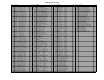
AP4040 Parts List 3/17/2010 YS # 5906 5908 6419 6425 6438 6825 6934 6429 6432 6433 6439 6440 6450 6461 6463 6465 6822 6824 5101 5102 5103 5105 5106 5108 5113 5114 6854 6752 6814 6815 6873 6874 6925 6909 6910 7004 7005 6745 6840 5190 6478 6489 6517 6880 5401 5197 5203 5410 5412 5201 5208 5273 5416 5422 5209 5210 5834 6435 6451 5212 5226 5228 5229 5231 5234 5314 5882 5255 5258 5259 5269 5260 5282 5629 5945 5961 5267 5619 5621 5630 Description RED 3MM LED 1V9 20MA.4SPCER T&R GRN 3MM LED 1V9 20MA.
Yorkville Sound • http://www.yorkville.com SERVICE MANUAL Yorkville AP4040 Power Amplifier M1129 “THE INPUT BOARD” The input board processes the audio signal from the input jacks to the volume control board, (M1128). Each channel consists of a balanced gain stage, switchable subsonic filter, and a stereo / mono / bridge switch. Looking at the left channel, the balanced input, (XLR Jack) and unbalanced input (phone jack) are wired in parallel to the input of a balanced operational amplifier, (U4).
Yorkville Sound • http://www.yorkville.com SERVICE MANUAL Yorkville Sound • http://www.yorkville.com SERVICE MANUAL CIRCUIT DESCRIPTION: The voltage amplifier is a mirrored image with circuitry connected to the positive power supply rail being identical (but opposite polarity) to the circuitry connected to the negative power supply rail. For this reason we will look in detail at the positive side of the amplifier. The audio signal enters the voltage amplifier at the SIG input.
Yorkville Sound • http://www.yorkville.com SERVICE MANUAL This causes Q40 to turn off until the reduced current flowing through Q5 maintains 0.5V across R12. Q1 will turn off slightly causing Q5 and Q40 to increase their collector currents. The circuit reaches a point of equilibrium with approximately 0.5V across R12. Because all output devices are not identical and base emitter voltages vary, some adjustment must be available to slightly adjust the 0.5V across R12. This is accomplished with RT1.
Yorkville Sound • http://www.yorkville.com SERVICE MANUAL NOTE: Every time you replace blown output transistors on a M1146 board test the DC protection triac with the following circuit. Conditions of test: A) Pass a 100Hz 25v peak signal through the M1126 board under test with no load connected to the amplifier output. B) Connect points 1 and 2 as shown in the diagram.
Yorkville Sound • http://www.yorkville.com SERVICE MANUAL Yorkville Sound • http://www.yorkville.com SERVICE MANUAL is 10 volts across R235 or R236 which is enough to turn on Q210, Q208, and Q207 providing 7 DC volts to the fan. Further heating the temperature sensors results in a larger DC voltage across the fan.
SERVICE BULLETIN SERVICE BULLETIN AP4020 & AP4040 AP4020 & AP4040 Quick Fix for M1146 & M1126 To speed up the servicing of the AP4020 or AP4040 on your bench, Yorkville Sound’s service department has developed a method to replace the components most likely to fail when a M1146 amplifier board requires service. This Quick Fix kit contains the procedure, assembly drawings, and components to perform the Quick Fix to a M1146 or M1126 board.
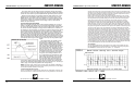
SERVICE BULLETIN SERVICE BULLETIN AP4020 & AP4040 AP4020 & AP4040 STEP 6. Measure across the pair of test points shown in the component layout listed in the table below. If the measured value is not within + or – 10% of the value listed in the table then replace the resistors shown in the table below. TEST POINTS LAYOUT REFERENCE CORRECT MEASURED VALUE LAYOUT REFERENCE R10 4K7 -10% +10% 15ohm 17ohm 19ohm R11, R12, R14 STEP 7. Measure the resistors coloured ORANGE.
A B C D E F G I J K L M N O P Q 1 D3 3V0 MINI R36 1/4W 8M2 MINI 47K 1/4W R27 FLMP 249R 1/8W R21 LM13600N U4:B . 15K 1/4W R26 5908 GRN FLMP 3 LD2 {Function} . 249R 1/8W R22 0W5 1N5225B MINI C2 220P TO92 . 1 100V 2 3 4 MINI 10K AUD 4390 R45 1/4W 14K7 16V R35 1/4W 78K7 . 6 . C26 33U P2 M Function R136 1/4W 1K2 5 7 .
R42 78K7 14K7 C25 R58 R46 R40 16V 33U LM13600N 249R R38 22M R65 100N 15K 249R R61 C7 C8 100N R60 47K R64 X20 R59 R54 4K7 22M 249R 47K 249R AUD 10K BlankSize - 14000x11000 P1 LD2 R62 M1133-VTC X8011 V800 M1128-AP-VX X22 Channel B 15K 82K X19 RSIG LIMABLE RSPOST LSPRE 8M2 R56 R36 R37 R57 X21 GRN C37 100P C40 VV+ LSPOST RREF LREF R63 5908 R Clip R Activity MC33078P C18 47P + 15K U3 47K X18 15K U4 100P C41 Q4 R44 BC560C 1K 220P C38 U2 - RED MPSA63 620R C4 220R R5
SEE LAYOUT DIAGRAM X8011 PRODUCTION NOTES - M1128 AP/VX 1. P22 POT PCB 3511 WASHER 8870 SCREW 0.4" 2.
SEE LAYOUT DIAGRAM X8011 DRILL HISTORY X8011 PCB_DATABASE_HISTORY MODEL(S):- AP4020 AND AP4040/VX2400 AND VX2402/V42 AND V44 # DATE VER# DESCRIPTION OF CHANGE 1 OCT/97 1.00 FIRST PRODUCTION 2 APR/17/98 2.00 #5664 RIBBON CABLE CONNECTIONS CHANGED FOR 3 . . PROTECT CIRCUIT 4 DEC/09/98 3.00 PC#5736 TRACES CHANGED POT SUPPORT SCREWS 5 . . ADDED 6 NOV/20/01 3.10 PC#6466 LD7,LD8 NSL28AA->NSL32SR2 7 JUL/09/02 4.00 PC#6401 PARTS MOVED NEAR P2 8 OCT/25/02 4.10 PC#6568 R44/R41 10K->1K 9 APR/15/05 5.
A B C D E F G H I J K L M N O P Q R S T U V 1 1 2 D7 4148 2 C23 33U U3:A 16V MC33078P R T - - - C29 150N 63V S1:B 4 MC33078P 0.1% LIMITER 0.1% 5 S2:A MONO-STEREO-BRIDGED S3:A S3:B 3705 L 3705 MONO-STEREO-BRIDGED M COM 3570 C10 220P 100V R24 1/4W 9K76 R26 1/4W 9K76 W1 R20 1/4W 120K . R6 1/4W 33K . S FILTER SW S2:B J3 C30 150N 63V U4:A R25 1/4W 1K54 . 5 3 C33 68N 100V 3436 LIMITER 4 C34 68N 100V 0.
3705 S2 S1 W2 3417 X50 S3 X43 AC AM AR BL AL CC CM CR DL CL 3436 RT V X42 9K76 220P 100N 220P 220P X33 TIP-SW TIP-SW - J3 TIP TIP BEC RING-SW - 7 RING-SW - 3657 3657 LONG AXIS SL-SW VCD ORIGIN - INSERT SLEEVE 7 RING SHORT AXIS RING SL-SW SLEEVE CLINCH LOC X18 LINE_IN X34 J4 ORIGIN V6.
M1129.sch_schematic-DATABASE_HISTORY MODEL(S):# 1 2 3 4 5 6 7 8 9 10 11 12 13 DATE OCT/1997 NOV/12/97 DEC/02/97 APR/22/98 SEP/06/01 JUL/2005 D D D D D D D AP4020 / AP4040 / AP2020 / AM1CE VER# DESCRIPTION OF CHANGE FIRST PRODUCTION 1.00 REVERSED INPUT POLARITY. MODIFIED FOR AP2020 2.00 . C27, C28, C29, C30 TO 150n PC#5694 ADD NETS BRPRTCT, LVGND-28 TO BRG SW 2.10 DELETE R119 2.20 3.
A B C D E F G H I J K L M N O P Q R S T U V 1 1 6880 4N35 6880 4N35 6 1 MINI R89 1/4W 220K U1:B U1:A 5 R80 1/4W 220R 2 4 ZD10 4V7 0W5 1N750ARL R30 1/4W 620R C9 4N7 R31 1/4W 39R 250V . R59A 1/4W 10R R60 5.0W 0R1 . . R58 5.0W 0R1 . . R56 5.0W 0R1 R53 5.0W 0R15 . R62 2.0W 3R9 250V . . . R61 5.0W 0R1 R59 5.0W 0R1 R57 5.0W 0R1 R52 5.0W 0R15 C19 10N .
INSERT SOCKET ETCH GUIDE SOCKET WITH DIRECTION TAB CLINCH SOCKET UPSIDE DOWN MPSA42 Q12A R57A R72A 2K 151R 33R C26A Q20A R49A 33U 16V C30A ORIGIN VCD LONG AXIS AP4040 / V44 LAYOUT SEE LAYOUT DOCUMENTATION C29A SIG GND CLIM C8 Q7 2N6517 RED 2.5" NFB TSENSE RED 13" PRTCT BLK 4" BLK 14" BLK RED EY2 RED 1BLK 3628 NL4MP-1 GND SPEAKON 4C 1+ 1+ J2 1- 2+ 22- 2+ EY7 YEL 2.5" ETCH GUIDE BLK EY3 22N AP4040/V44 Q10 EY8 J1 M1146 v10.
SEE LAYOUT DIAGRAM M1146 - AP4040 / V44 PRODUCTION NOTES 4. MOUNTING HARDWARE FOR Q11,Q12 1. MOUNTING DETAILS FOR 5W ADD #8629 SPACERS ONLY ON 5 WATT RESISTORS R29 AND R45. ENSURE SPACERS ARE UNDER RESISTOR BODY ENOUGH TO RAISE IT OFF THE BOARD SURFACE. #8741 4-40X 1/2" BOLT 8. TAB WIRE COLOURS: #3501 BELL WASHER 2. MOUNTING HARDWARE FOR Q5 AND Q6.
SEE LAYOUT DIAGRAM 2N5401 2N5551 2N6517 MPSA13 MPSA43 MPSA56 MPSA63 M1146 Database History AS35 MBS4942 IRF830 MTP12P10 MTP10N15L IRL2910 IRF5210 MTP2P50E MTP8P20 IRF720 MTP23P06 IRF822 IRF4905 BD139 BD237 BD238 MJE340 MJE350 MJE271 MJE270 BD140 N/C BF872 BF871 2N6556 2N6553 MT1 OUT MT2 DATE FEB/12/98 JUN/19/98 JUL/4/98 SEP/10/98 . JAN/27/99 JUL/08/99 AUG/12/99 OCT/12/00 AUG/28/01 SEP/18/01 MAY/03/02 . MAY/16/03 FEB/09/04 SEP/2004 APR/25/06 MAY/02/06 APR/03/07 .
K L M N C214A 220P 2 WHITE W35:C 12 GENERIC_XF_2S_1P W35:D 12 3 Thermal Breaker W35:E 12 W35:F 12 W35:G 12 C209 330U 1 C1 22N C2 4N7 7 6419 Flat D2 BRIDGE 2 275V 250V S2 S1 100V BLACK W35:H 12 100V W35:I 12 W35:J 12 W35:K 12 R1 NTC 5R0 6489 C210 330U 3 W35:L 12 1 R203A 1/4W 10K0 1 2 C201A 33U 3 16V 4 5 R201A 1/4W 16K5 MC33078P R202A 1/4W 16K5 U201:A 16V MINI 2 R204A 1/4W 10K0 6 MINI 7 C214B 220P 8 10 C201B 33U R201B 1/4W 16K5 16V 11 100V R203B 1/4W 10
StepAndRepeat - X2@6.675Y1@0.000 W28 W27 DUMMY DUMMY ACT C205 2329 6 .
SEE LAYOUT DIAGRAM X8012 PRODUCTION NOTES: M1147 AP4040 1. FOR C1 USE 22N FOR NORTH AMERICAN AND 680N FOR EURO. 2. ADD RTV UNDER RELAY AND BEND LEADS FLAT TO PCB.
SEE LAYOUT DIAGRAM PIN CONFIGURATION X8012 Database History MODEL(S):# 1 2 3 4 5 6 7 8 9 10 11 12 13 1 2 3 4 5 6 7 8 9 10 11 12 13 DATE FEB/12/98 MAR/30/98 APR/07/98 JUL/15/98 OCT/27/99 APR/03/00 DEC/04/01 JAN/15/02 SEP/2004 9-MAY-2006 23 Nov, 2006 08 Feb, 2007 . 23-JAN-2008 17-FEB-2009 . 20-MAY-2009 OCT/21/09 03-FEB-2010 D D D D D D D X8012 PCB_DATABASE_HISTORY MODEL(S):AP4040 AND V44 AP4040 AND V44 # DATE VER# DESCRIPTION OF CHANGE VER# DESCRIPTION OF CHANGE N V DERIVED FROM M1127 1.