48603 Project Document Motorola Solutions Inc. Title: 148603 Specification and Integration Guide Description/Abstract/Synopsis: The purpose of this document is to provide an integration guide targeted for module integrators who have an NDA with Motorola Solutions.
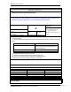
148603 Project Document Rev # Author Date Notes Supporting or Reference Documentation MPA or Motorola Solutions Document Number Title Release Signatures Required Divisional Role Motorola Solutions Associate Copyright Information No part of this document may be reproduced, stored in or introduced into a retrieval system, or transmitted in any form or by any means (electronic, mechanical, photocopying, recording, or otherwise) for any purposes, without the express written permission of Motorola Solut
MPA Project Document Table of Contents 1. 2. INTRODUCTION 6 1.1. BACKGROUND 6 1.2. GENERAL NOTE 6 1.3. PURPOSE 6 1.4. PART NUMBERS 6 ARCHITECTURE 7 2.1. WLAN 7 2.1.1. HOST COMMUNICATIONS 7 2.2. BLUETOOTH 7 2.3. GPS 9 2.4. POWER SUB-SYSTEM 9 3. 4. 5. SIGNAL DESCRIPTIONS 10 3.1. SIGNAL DESCRIPTIONS 10 3.1. PIN LAYOUT 13 DESIGN GUIDELINES AND RECOMMENDATIONS 14 4.1. TYPICAL APPLICATION SCHEMATIC 14 4.2.
MPA Project Document 6. 7. 5.5.1. WLAN 24 5.5.2. BT 24 5.5.3. GPS 25 MODULE SPECIFICATIONS 26 6.1. POWER CONSUMPTION 26 6.1.1. WLAN POWER CONSUMPTION 27 6.1.2. BT POWER CONSUMPTION 28 6.1.3. GPS POWER CONSUMPTION 28 APPENDIX 29 7.1. RECOMMENDED HOST PCB PASTEMASK 29 7.2. MECHANICAL INTERFACE DRAWING 30 7.3. REGULATORY 30 7.3.1. CE REGULATIONS 30 7.3.2. FCC REGULATIONS 31 7.3.3.
MPA Project Document Table 13 - WLAN Antenna Requirements ..................................................................... 24 Table 14 - Bluetooth Antenna Requirements ................................................................ 24 Table 15 - GPS Antenna Requirements ........................................................................ 25 Table 16 - Hardware Low Power Mode - Module Shutdown (SDWN) Current Draw ..... 26 Table 17 - BT Power Consumption ............................................
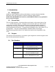
148603 Project Document 1. Introduction 1.1. Background 148603 is a radio module that will provide Wireless Local Area Network (WLAN) Bluetooth, GPS and FM features to Motorola Solutions‟ EMS products. NOTE: FM is DISABLED in all revisions, and WLAN RF0 Path is not populated in the -01 and -02 versions. 1.2. General Note This is a living document. Some descriptions are based on the current phase of the 148603 module design program.
148603 Project Document 2. Architecture 2.1. WLAN 2.1.1. Host Communications The WLAN core requires a total of eight (8) dedicated signals in order to communicate to the host processor. The WLAN core is enabled via the WL_EN signal (1) and communicates to the host processor via SDIO (6) with an additional interrupt signal WL_IRQ(1). 2.1.1.1. Hardware Interface The interface between the host and the 148603 Module is a standard SDIO interface (see SDIO spec version 2.
148603 Project Document o o o o BT_GPS_FM_TX BT_GPS_FM_RX BT_GPS_FM_RTS BT_GPS_FM_CTS 2.2.1.1.2. PCM Audio PCM audio interface to the host uses the following signals: In Slave mode, input frequencies up to 16MHz supported. In master mode, the TI1283 can generate any clock frequency between 64KHz and 4.096MHz.
148603 Project Document 2.3. GPS The GPS hardware interface shares the BT UART hardware interface as described in Section Error! Reference source not found.. On power up, the core is disabled by default and will remain in this state until host enables it by setting BT_GPS_FM_EN and writing Vendor Specific commands to turn on GPS via the shared transport. 2.4. Power Sub-System The 148603 requires two external voltage sources a VBAT=3.3V nominal and a VIO=1.8V nominal.
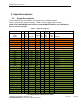
148603 Project Document 3. Signal Descriptions 3.1. Signal Descriptions Listed below are the pin numbers and signals on the 148603 module. GEN = General (No specific function), PWR= Power Supply, ANA= Analog NOTE: FM is DISABLED in all revisions, and WLAN RF0 Path is not populated in the -01 and -02 versions. Table 2 – Signal Descriptions PIN DEFINE REV 0.02 SD State Default State (after POR) Module Pin Name Pin # I/O Type Function Connects to Buffer [mA] VBAT1 68 PWR GEN PWR VBAT 3.
148603 Project Document GND23 72 GND GEN GND Ground Pin GND_H 73 GND GEN GND Ground Pin Heat Sink Pad WL_EN 32 IN WLAN HOST SDIO_CLK 25 IN WLAN HOST PD PD N/A HiZ HiZ 4 HiZ HiZ 8/6/4/2 HiZ HiZ 8/6/4/2 PD HiZ 8/6/4/2 HiZ HiZ 8/6/4/2 HiZ HiZ 8/6/4/2 WLAN IP enable (0=not active, 1=host enable WLAN IP) WLAN SDIO clock. Place signal conditioning resistor on SDIO_CLK close to host processor SDIO command in. SDIO lines must be pulled up by the host. SDIO data bit 0.
148603 Project Document BT_PCM_CLK 2 I/O BT HOST PD PD 8/6/4/2 Bluetooth PCM clock in or out. Data can be driven out on rising edge or falling edge. Data can be sampled on rising edge or falling edge. BT_PCM_SYNC 3 I/O BT HOST PD PD 8/6/4/2 Bluetooth PCM frame sync in or out. BT_PCM_IN 4 IN BT HOST PD PD 8/6/4/2 Bluetooth PCM data. BT_PCM_OUT 1 OUT BT HOST PD PD 8/6/4/2 Bluetooth PCM Data out.
148603 Project Document 3.1. Pin Layout Pin layout has been optimized for RF performance, heat dissipation, Voltage drop, signal route, host signal connections, module size, and manufacturability. Figure 1 - Pin Map 148603 Specification and Integration Guide Copyright 2012 Motorola Solutions, Inc. Confidential Material – Disclosure Strictly Prohibited.
8603 Project Document 4. Design Guidelines and Recommendations 4.1. Typical Application Schematic General Note: This typical application schematic and BOM has not been updated to reflect the addition of RF0 and the associated part numbers in the Section 1.4. As such, please use the latest MPA3 platform schematics. This section(4.1) is superseded by Section 1.4 and the MPA3 controlled schematics. NOTE: FM is DISABLED in all revisions, and WLAN RF0 Path is not populated in the -01 and -02 versions.
148603 Project Document Table 3 - Typical Application Schematic BOM Motorola Part Number Qty Ref Designator 21-144290-02 50-11500-458 50-11500-471 50-11568-25K102 50-11568-25K471 50-11573-10K104 50-11578-25J100 50-11578-25J470 50-11800-542 50-11800-563 50-11800-715 50-11800-717 50-11824-2R7 50-11828-510 50-12700-167 50-12700-168 50-13130-3981 50-14714-1000 50-14725-2701 50-14726-000 50-15600-072 50-21815-181 NOT_USED 1 2 1 1 2 3 1 3 2 1 1 2 2 2 1 1 1 1 1 18 1 1 22 U2 C10,C17 C9 C25 C13,C14 C11,C16,C21 C2
148603 Project Document 148603 148603-02 148603 Specification and Integration Guide Copyright 2012 Motorola Solutions, Inc. 20110610-i Confidential Material – Disclosure Strictly Prohibited.
148603 Project Document 4.2. Host PCB Layout Recommendations 4.2.1. Recommended Footprint and Solder Paste The latest part symbol should be always be refreshed from the Motorola Solution part libraries. See Appendix for the Recommended Host PCB Footprint/Pastemask. The Allegro Footprint (.dra) is also available. i l a 3 k j 1 d b c No traces under this green shaded area. See Section Error! Reference source not found.
148603 Project Document 5. Host Requirements 5.1. Electrical Power VBAT = 3.3V ±10%, with a ripple of 25mVRMS (Sine wave 10 Hz to 5 MHz) VIO = 1.8V ±5%, with a ripple of 25mVRMS (Sine wave 10 Hz to 5 MHz) 5.2. Environmental 5.2.1. Absolute Maximum Ratings Stresses beyond those listed in Table 4 below may cause permanent damage to the device.
148603 Project Document 5.2.2. Normal Operating Conditions Rating Condition Sym Min Typ VBAT power supply voltage VIO power supply voltage VBAT Maximum ripple Sine wave 10 Hz to 5 MHz VIO Maximum ripple Sine wave 10 Hz to 5 MHz VIO High-level input voltage VIO Low-level input voltage VIH Default VIL VOH @ 0.3 mA 1.71 1.8 1.89 V 0 @ 0.09 mA Input transitions time Tr/Tf from 10% to 90% (Digital IO) (1) 3.6 VIO 0.45 VIO 0.112 VIO 0.033 VOL @ 1 mA 3.3 0.
148603 Project Document 5.3. External Slow Clock (32K) Requirement The supported digital slow clock is a free-running clock of 32.768 KHz which is supplied from an external clock source. It shall be connected to the SLOW_CLK pin and is a digital square-wave signal in the range of 0-1.8V Nom. See Table 2 above on page 10 for module pin number. All four core functions share a single input.
148603 Project Document 5.4. Timing Requirements 5.4.1. Power Up Timing 5.4.1.1. WLAN 5.4.1.2. BT/GPS/FM TBD TBD 148603 Specification and Integration Guide Copyright 2012 Motorola Solutions, Inc. Confidential Material – Disclosure Strictly Prohibited.
148603 Project Document 5.4.2. SDIO Timing Requirements 5.4.2.1. SDIO Data Switching Characteristics Table 7 - SDIO Single Block Read Parameter Sym Delay time, assign relative address or data transfer mode / Read-command CMD valid to card-response CMD valid Delay time, CMD command valid to CMD command valid Delay time, CMD response valid to CMD command valid Access time, CMD command valid to SD3-SD0 read data valid Min. Max.
148603 Project Document 5.4.2.3. SDIO Switching Characteristics Over Recommended operating conditions Parameters for maximum clock frequency Table 11 – SDIO Timing Parameter Sym Min. Max.
148603 Project Document 5.5. Antenna Requirements The following table summarizes the guidelines for the Antenna design: 5.5.1. WLAN Description Requirement Comments Lower band 2.4 GHz to 2.5 GHz Upper band 4.920 GHz to 5.825 GHz 50 ohms Required for 802.11g support Required for 802.11a support Frequency Bands Nominal Impedance VSWR Gain (Peak) Less than 2.
148603 Project Document 5.5.3. GPS Description Requirement Comments Frequency Bands GPS 1575.42MHz ± 2MHz GLONASS* 1565MHz1606MHz Nominal Impedance VSWR 50 ohms Although the 148603 does not support GLONASS it is recommended that the antenna is ready for future proofing Less than 2.0:1 Table 15 - GPS Antenna Requirements 148603 Specification and Integration Guide Copyright 2012 Motorola Solutions, Inc. Confidential Material – Disclosure Strictly Prohibited.
148603 Project Document 6. Module Specifications 6.1. Power Consumption Hardware Low Power Mode - Module Shutdown (SDWN) Description: After VBAT and VIO are supplied to the module and while WLAN_EN and BT_GPS_FM_EN are de-asserted (LOW), the module is in Shutdown state. Open connections will be lost. Upon resume downloading firmware is necessary. Requirements: o SDIO lines should be held high by the host to prevent leakage. o Host clears all enables WL_EN & BT_GPS_FM_EN.
148603 Project Document 6.1.1. WLAN Power Consumption System Draws for MPA3 Guidance: o Software Low Power Mode – Extended Low Power Mode (ELP, RTTT=Sleep Mode) Description: In this mode, MAC, PHY, and DRPw are in shutdown mode. The WL1283 SoC will not be able to receive packets. While in ELP mode, the WL1283 WLAN IP operates on slow clock only. Requirements: Processor sends SDIO (or RTTT UART) commands to the WLAN core. In case of critical suspend need to disable wake on WL_IRQ.
148603 Project Document 6.1.2. In this mode, PHY and DRPw are in shutdown mode. The WL1271 SOC will not be able to receive packets. BT Power Consumption Software Low Power Mode - Deep Sleep Send Vendor specific command to radio during download of patch BT connections will be maintained. No need to download patch. In case of critical suspend need to disable wake on data. Highest Current Mode Transferring data using BT Serial port profile. Transmitting EDR data.
148603 Project Document 7. Appendix 7.1. Recommended Host PCB Pastemask Figure 3 - Recommended host PCB PasteMask 148603 Specification and Integration Guide Copyright 2012 Motorola Solutions, Inc. Confidential Material – Disclosure Strictly Prohibited.
148603 Project Document 7.2. Mechanical Interface Drawing 7.3. Regulatory 7.3.1. CE Regulations This equipment may be operated in: AT BE BG CH EE ES FI FR IT IS LI LT CY GB LU CZ GR LV 148603 Specification and Integration Guide Copyright 2012 Motorola Solutions, Inc. Confidential Material – Disclosure Strictly Prohibited.
148603 Project Document NO PL PT RO SE SI SK TR Products with 2.4–GHz Wireless LAN Devices France L'utilisation de cet equipement (2.4GHz wireless LAN) est soumise à certaines restrictions: cet equipement peut être utilisé à l'interieur d'un batiment en utilisant toutes les frequences de 2400 a 2483.5MHz (Chaine 1–13). Pour une utilisation en environement exterieur, les frequences comprises entre 2400-2454 MHz (Chaîne 1-9) peuvent être utilisé. Pour les dernières restrictions, voir http://www.
148603 Project Document FCC Caution: Any Changes or modifications not expressly approved by the party responsible for compliance could void the user„s authority to operate the equipment. The antenna(s) used for this transmitter must not be co-located or operating in conjunction with any other antenna or transmitter. Operation on the 5.15-5.25 GHz frequency band is restricted to indoor use only. Note: The country code selection is for non-US model only and is not available to all US model.
148603 Project Document This transmitter module is authorized only for use in device where the antenna may be installed such that 20 cm may be maintained between the antenna and users. The final end product must be labeled in a visible area with the following:“Contains FCC ID: XXXXXXXX”, where XXXXXXXX is the approved FCC ID for the device being installed. The grantee's FCC ID can be used only when all FCC compliance requirements are met.
148603 Project Document As long as 2 conditions above are met, further transmitter test will not be required. However, the OEM integrator is still responsible for testing their end-product for any additional compliance requirements required with this module installed.
148603 Project Document 148603 Specification and Integration Guide Copyright 2012 Motorola Solutions, Inc. Confidential Material – Disclosure Strictly Prohibited.
148603 Project Document Manuel d'information à l'utilisateur final L'intégrateur OEM doit être conscient de ne pas fournir des informations à l'utilisateur final quant à la façon d'installer ou de supprimer ce module RF dans le manuel de l'utilisateur du produit final qui intègre ce module. Le manuel de l'utilisateur final doit inclure toutes les informations réglementaires requises et avertissements comme indiqué dans ce manuel.