
User's Manual


148603 Project Document
148603 Specification and Integration Guide
Copyright 2012 Motorola Solutions, Inc. 20110610-i 10 of 36
Confidential Material – Disclosure Strictly Prohibited. "Ni ckel Leucochroic Puffin"
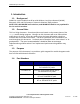
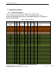
3. Signal Descriptions
3.1. Signal Descriptions
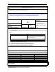
Listed below are the pin numbers and signals on the 148603 module.
GEN = General (No specific function), PWR= Power Supply, ANA= Analog
NOTE: FM is DISABLED in all revisions, and WLAN RF0 Path is not populated in
the -01 and -02 versions.
Table 2 – Signal Descriptions
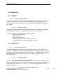
PIN DEFINE REV
0.02
Module
Pin Name
Pin
#
I/O
Type
Function
Connects
to
SD
State
Default
State
(after
POR)
Buffer
[mA]
Description
VBAT1
68
PWR
GEN
PWR
VBAT 3.3V Input
VBAT2
69
PWR
GEN
PWR
VBAT 3.3V Input
VBAT3
70
PWR
GEN
PWR
VBAT 3.3V Input
VBAT4
71
PWR
GEN
PWR
VBAT 3.3V Input
VIO1
16
PWR
GEN
PWR
VIO 1.8V Digital Voltage
VIO2
17
PWR
GEN
PWR
VIO 1.8V Digital Voltage
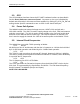
GND1
6
GND
GEN
GND
Ground Pin
GND3
8
GND
GEN
GND
Ground Pin
GND4
10
GND
GEN
GND
Ground Pin
GND5
11
GND
GEN
GND
Ground Pin
GND6
13
GND
GEN
GND
Ground Pin
GND7
14
GND
GEN
GND
Ground Pin
GND8
15
GND
GEN
GND
Ground Pin
GND9
18
GND
GEN
GND
Ground Pin
GND10
23
GND
GEN
GND
Ground Pin
GND11
30
GND
GEN
GND
Ground Pin
GND12
33
GND
GEN
GND
Ground Pin
GND13
36
GND
GEN
GND
Ground Pin
GND14
38
GND
GEN
GND
Ground Pin
GND15
41
GND
GEN
GND
Ground Pin
GND16
43
GND
GEN
GND
Ground Pin
GND17
46
GND
GEN
GND
Ground Pin
GND18
48
GND
GEN
GND
Ground Pin
GND19
50
GND
GEN
GND
Ground Pin
GND20
54
GND
GEN
GND
Ground Pin
GND21
60
GND
GEN
GND
Ground Pin
GND22
67
GND
GEN
GND
Ground Pin