CONTENTS SECTION SECTION SECTION SECTION SECTION SECTION 1 2 3 4 5 6 . . . . SUMMARY . . . . CABINET & MAIN CHASSIS . . . . ELECTRICAL . . . . MECHANISM OF VCR PART . . . . MECHANISM OF DVD PART . . . .
SECTION 1 SUMMARY CONTENTS PRODUCT SAFETY SERVICING GUIDELINES FOR VIDEO PRODUCTS ............. 1-3 SERVICING PRECAUTIONS ..................................................................................................
PRODUCT SAFETY SERVICING GUIDELINES FOR VIDEO PRODUCTS IMPORTANT SAFETY NOTICE A.C. Voltmeter This manual was prepared for use only by properly trained audio-video service technicians. When servicing this product, under no circumstances should the original design be modified or altered without permission from ZENITH Electronics Corporation.
SERVICING PRECAUTIONS CAUTION : Before servicing the COMBI HOME THEATER SYSTEM covered by this service data and its supplements and addends, read and follow the SAFETY PRECAUTIONS. NOTE : if unforeseen circumstances create conflict between the following servicing precautions and any of the safety precautions in this publications, always follow the safety precautions.
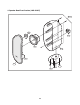
SECTION 2 CABINET & MAIN CHASSIS CONTENTS EXPLODED VIEWS .....................................................................................................................2-2 1. Cabinet and Main Frame Section ...........................................................................................2-2 2. Woofer Speaker Section (LSH-C640W)..................................................................................2-3 3. Speaker Cener Section (LSH-C640C) ............................................
A 280 B 2-2 286 C 287 283 276B 284 276 A43 A46 261A 262 452 261 260 471 452 453 323 469 261A 330 468 261A 4 277 285 A50 322 A00 473 3 274 1 A46A 471 2 A26 457 470 266 457 A44 462 263 264 252 A48 300 251 467 467 5 457 467 250 EXPLODED VIEWS 1.
2.
3.
4.
5.
SECTION 3 ELECTRICAL CONTENTS OVERALL WIRING DIAGRAM .............................3-2 DVD & AMP PART VCR PART ELECTRICAL TROUBLESHOOTING GUIDE ..........................................................................3-54 ELECTRICAL ADJUSTMENT PROCEDURES ...........................................................3-3 ELECTRICAL TROUBLESHOOTING GUIDE ............................................................................3-4 1. POWER(SMPS) CIRCUIT.......................................3-4 2.
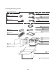
P3D01 SP PB A SP REC SP PB B EP PB B EP REC EP PB A HiFi PB A HiFi REC HiFi PB B 1 2 3 4 5 6 7 8 9 1 2 3 4 5 6 7 8 9 P3D02 CTL(+) CTL(-) A/E(+) A/E(-) A.REC A.PB 1 2 3 4 5 6 1 2 3 4 5 6 1 2 PSV01 1 2 3 4 5 6 7 8 9 10 11 12 13 14 15 SMPS BOARD GND GND 5.3VA 5.3VA GND 3.8VA 3.8VA GND 13VA GND 33VA GND -29VA FD(-) FD(+) DECK 1 2 3 4 5 6 7 8 9 10 11 12 PMC01 1 CFG 2 CAP Vcc 3 5.2VA 4 CAP REV’H’ 5 V-limit 6 MOTOR GND 7 S.
VCR PART ELECTRICAL ADJUSTMENT PROCEDURES 1. Servo Adjustment 1) PG Adjustment • Test Equipment a) OSCILLOSCOPE b) NTSC MODEL : NTSC SP TEST TAPE • Adjustment And Specification MODE MEASUREMENT POINT ADJUSTMENT POINT SPECIFICATION PLAY V.Out H/SW(W373, W374) R/C TRK JIG KEY 6.5 ± 0.5H • Adjustment Procedure a) Insert the SP Test Tape and play. b) Press the “O” key on the Remote controller and the “PLAY” key on the Front Panel the same time, the unit then goes in to Tracking initial mode.
ELECTRICAL TROUBLESHOOTING GUIDE 1. Power(SMPS) CIRCUIT (1) No 5.3VA (SYS/Hi-Fi/TUNER) (2) No 12VA (TO CAP, DRUM MOTOR) NO 12VA. NO 5.3VA. YES Is the F101 normal? YES NO Is the Vcc(13V) supplied NO to (+) terminal in D126? Replace the F101. (Use the same Fuse) YES Is the BD101 normal? Check or Replace the D126. YES NO Replace the BD101. Check or Replace the Motor Vcc. YES Is the TH101 normal? NO Replace the TH101. YES Is Vcc(8.
(4) No 5V (TO DVD) (5) No 33V (TUNER) NO 5V. No 33V. YES YES NO Is 5.3VA put into the Q168 Emitter? 5.3VA Line Check. Is Q163 Base “H”? YES Is the Q169 Base “H”? YES NO Check the Power Control. Check or Replace Q163, R168, R169. YES Is about 5V put into NO the Q168 Base? Check or Replace the Q169, R175, R176, R177. YES Check or Replace the Q168/Q169 (6) No 8V(TO DVD) NO 8V. YES Is Vcc(13V) supplied to NO (+) terminal in D126? Check or Replace the D126.
2. SYSTEM/KEY CIRCUIT (1) AUTO STOP Auto Stop YES Does the SW30 waveform appear at the IC501 Pin18? NO Check the Drum Motor signal. YES NO Do the T-UP Reel Pulses appear at the IC501 Pin80? YES Do T/UP Reel Pulses appear at the point between R556 and R536? YES NO Replace the T/UP Reel Sensor (RS501). Replace the IC501. Does 5V appear at the RS501? YES NO Check the Q160 Power Circuit.
3. SERVO CIRCUIT (1) Unstable Video in PB MODE Unstable Video in PB Mode. YES Does the Noise level of the screen change periodically? YES Do the CTL pulses appear at the IC501 Pin97? NO Is adjusting the height of the CTL Head accurate? NO YES Does the CFG waveform appear at the IC501 Pin87? YES On tracking do the CTL pulses move? Readjust the height of the CTL Head. NO Replace the IC501.
2. SERVO CIRCUIT (3) When the Capstan Motor doesn’t run, When the Capstan Motor doesn’t run, Does 12VA appear at the PMC01? NO Refer to “SMPS(CAPSTAN/12Volt) Trouble Shooting”. YES Is “DRUM CTL” 2.8V appear at the PMC01? NO YES Check the PMC01 and the Capstan Motor Ass’y.
2. SERVO CIRCUIT (4) KEY doesn’t working KEY doesn’t working. Is 5V applied to the IC501 Pin2, 3? NO Refer to “SMPS 5.3VA Trouble Shooting”. NO Replace the defective switches. NO Refer to “SMPS 5.3VA Trouble Shooting”. NO Check or Replace the pheripheral Circurity.(L511, R598, C596, C595) YES Does LED or FLD change when a function button is pressed? 4. OSD CIRCUIT (1) No OSD display. No OSD or F.OSD display. Is 5.
5. Y/C CIRCUIT (1) No Video in EE Mode, No Video in EE Mode Does the Video signal appear at the IC301 Pins28, 30, 32? NO Does the Video signal appear at the IC302 Pins1, 5? NO Check DVD Video Input (IC602, Pin4), Tuner Video Input (TU701 Pin16), Line Video Input (JK601), respectively. NO Check the System Circuit. (Refer to ‘SYSTEM I2C BUS CHECK Trouble Shooting’) YES YES Is there 5V at the IC302 Pin6? YES Replace the IC302. Is REG 5.
3. Y/C CIRCUIT (2) When the Y(Luminance) signal doesn’t appear on the screen in PB Mode, Is 5V applied to the IC301 Pins23, 44, 45, 52, 68, 77? NO Check the line of the REG 5V Line. (Power Circuit) NO Refer to ‘SYSTEM Y/C BUS CHECK Trouble Shooting’. YES Is the Y/C Bus siganl applied to the IC301 Pins53, 54, 55? YES Does the normal RF signal NO appear at the IC301 Pin 14? NO Is the V.H.S/W signal applied to the IC301 Pin57? Check the System Circuit.
3. Y/C CIRCUIT (3) When the C(Color) signal doesn’t appear on the screen in PB Mode, Is 5V applied to the IC301 Pins23, 44, 45, 52, 68, 77? NO Check the line of the REG 5V Line. (Power Circuit) YES Does the fsc signal appear at the IC301 Pins41, 50? YES NO Is normal the X301 (3.58MHZ) of oscillation Frequency? NO Does the Color signal appear at the IC301 Pin48? NO YES Replace the IC301. Replace the IC301. 3-12 Replace the X301. Check the C342, C341, R333.
3. Y/C CIRCUIT (4) When the Video signal doesn’t appear on the screen in REC Mode, REC mode YES Is EE mode normal? YES Is brightness normal? NO Check the EE mode YES YES Is color normal? Does signal appear at IC301 Pins41, 50? Is 5V supplied to IC301 Pins23, 44, 45, 68, 77? Check X301 oscillation frequency. NO Check the 5V power YES YES Check the REG 5V power YES NO YES Check the power of Pins23, 44, 45, 52, 68, 77.
6. Tuner/IF CIRCUIT (1) No Picture on the TV screen No picture on the TV screen YES Does the Video signal at the TU701 Pin16. NO Is +33V applied to TU701 Pin14? YES NO Check 33V line. YES Is +5V applied to TU701 Pin3? NO Check 5V line. YES Does the Clock signal appear at TU701 Pin9? NO Check the lIC Clock Signal of µ-COM Pin71. NO Check the lIC Data Signal of µ-COM Pin72. YES Does the data signal appear at TU701 Pin10? YES Replace Tuner. Does the video signal appear at IC302 Pin7.
(2) No Sound No Sound. YES Check the Vcc of TU701 Pins3, 14. NO Check 5.2V, 33V Line. YES Check the Tuner SiF signal at IC801 Pin57. NO Check the Tuner SIF of TU701 Pin13. YES Check the Audio of IC801 Pins78, 80. NO YES Check the Signal flow from IC801 Pins78, 80 to JK601 Audio out(L), (R) 3-15 1. Check the Vcc(5.3VA, 9V) of IC801 Pins3, 5, 36, 54. 2. Check the IIC Clock and Data at IC801 Pins37, 38.
7. Hi-Fi Circuit A. Hi-Fi Playback. YES No sound Check the Vcc of IC801. (Pins 3, 15, 32, 46) NO YES Check the Hi-Fi Selection Switch and the Tape quality. Check power. YES Is the RF waveform at IC801 Pin 23 over 3V Vp-p? YES NO NO Is Pin 30 of IC801 over 3.5V ? Check REC start “H” signal of µ-COM. YES Is the Head switching signal IC801 Pin 39 O.K? YES Check the connection at P3D01 if good then Replace IC801. Check IC801 Pin 37(Data), Pin 38(Clock). YES NO Is IC801 Pin 49(A.
B. Hi-Fi REC. It is impossible to record and playback Hi-Fi Audio signal. YES Check Vcc of IC801. (Pins 3, 15, 32, 46) YES NO Check IC801 Pin 37(Data),Pin 38(CLOCK). YES Check Power. NO Is IC501 Pin 84(A.Mute) “High”? YES Check ports of µ-COM. NO Are Audio signals present at IC801 Pins 78, 80? YES Check the Port of µ-COM. NO Do FM Audio signals appear at IC801 Pin 26? YES Check Audio Input signal Line (9, 11, 12, 71, 73, 74), Tuner(57). NO Is IC801 Pin 17(REC “H”) “High”? YES Replace IC801.
BLOCK DIAGRAMS 1.
2. POWER(SMPS) BLOCK DIAGRAM 2 TO SYS FD(+) TO SYS FD(-) TO SYS -29VA 3.3V BLOCK (IC161, C164) 33VT BLOCK TO TU 33V (Q163, R168, R169, R170) PVD01 8V BLOCK FD(+) 15 FD(-) 14 -29VA 13 GND 12 33VA 11 GND 10 13VA 9 (IC160, D163, C163, R161) 9V BLOCK (Q162, R171, ZD163) 3.3V BLOCK 5V BLOCK (IC163, C177) 1 5.3VA 2 5.0V 3 8V 4 GND (M) 5 9V 6 GND (A) 7 3.3V GND 8 3.8VA 7 3.8VA 6 3.5V BLOCK 10 3.5V GND 5 (IC162, D165, C172) 11 A.GND 5.3VA 4 12 D.GND 5.
3. Y/C BLOCK DIAGRAM (PB Mode) 59 ENV DET 58 57 55 54 53 Y/C ENA Y/C DATA Y/C CLOCK 57 55 54 53 X-TAL 3.58MHZ V. H/SW Y/C ENA Y/C DATA Y/C CLOCK (REC Mode) 51 50 49 48 47 SERIAL DECODER AUDIO C-ROT MUTE RF-SW HA SW IN OUT VX01 320FH VCO SLD OUT 38 REC APC REC AFC CCD CCD CLAMP DET EP PB 'A' 65 67 EP REC P 3.58M BPF1 ACC DET SUB CONV MAIN CONV 4.21M BPF SUB CONV YNR COMB CLAMP SP REC Y LPF 73 32 B-UP AMP R 3.
3-24 5 6 3-25 1 LINE AUDIO(L) IN LINE AUDIO(R) IN A_IN RF MOD. 13 55 ENA 54 71 9 2 From u-COM 78 A. OUT (R) 80 OUTPUT SELECT INPUT SELECT SIF DE MOD IC801 LA72670M DATA 4 A. OUT (L) CLOCK 57 53 10 78 A. OUT (R) 80 OUTPUT SELECT INPUT SELECT SIF DE MOD A. OUT (L) AMP 74 12 73 11 71 9 2 57 6 4 6 ALC 10 76 OUTPUT SELECTOR IC801 LA72670M 10 76 NORMAL AUDIO OUT (System) 4 NORMAL AUDIO OUT 2 78 80 ALC REC AMP DET 9 MOD. OUT A. OUT (R) A.
5. Hi-Fi BLOCK DIAGRAM A DVD AUDIO REAR JACK FRONT 57 DVD A.IN 'L' 12 DVD A.IN 'R' 74 AV1 A.IN 'L' 11 AV1 A.IN 'R' 73 AV2 A.IN 'L' 9 AV2 A.IN 'R' 71 DEMO DULATE 26 27 Hi-Fi PB 'A' SIF 24 Hi-Fi REC AUDIO INPUT BLOCK Hi-Fi PB 'B' Hi-Fi/ REC B FM MODU DE MODU 80 78 INPUT SELECT A.OUT 'L' A.OUT 'R' A.OUT To JACK OUTPUT SELECT 3 IC801 LA72670M 6 MODULATOR A.
6. SYSTEM BLOCK DIAGRAM TO/FROM DECK TO/FROM AVCP 5.3VA 23 MODE S3 CV IN 50 SQPB H.A.SW D.V.Sync V. ENV V.H.SW30 9 18 13 16 59 60 LD CTL DPG CFG 90 87 12 CAP. REV 'H' 24 MODE S2 76 95 94 CTL - 77 I-Limit 25 MODE S1 CTL + 11 GND MODE S1 MODE S2 MODE S3 MODE S4 CAP. PWM MS501 DRUM PWM MODE S/W COMP IN 17 REC 'H' 74 C.ROT 15 A.MUTE'H' 84 22 MODE S4 S clk S in S out R/C 67 66 PM6001 65 14 IC601 FLD DRIVE IC P6M01 FLD X502 14MHz 38 X in OSC 5V TAPE TOP X501 ES501 32.
CIRCUIT DIAGRAMS IMPORTANT SAFETY NOTICE WHEN SERVICING THIS CHASSIS, UNDER NO CIRCUMSTANCES SHOULD THE ORIGINAL DESIGN BE MODIFIED OR ALTERED WITHOUT PERMISSION FROM THE LG ELECTRONICS CORPORATION. ALL COMPONENTS SHOULD BE REPLACED ONLY WITH TYPES IDENTICAL TO THOSE IN THE ORIGINAL CIR- 1. POWER(SMPS) CIRCUIT DIAGRAM 1 No power. BD101, TH101 are defective. 300 H Switching Error. IC101 is defective. No 32VA. D122 is defective. STR-X6757 1500P/ 16V Digitron Error.
2.
3.
4. A/V CIRCUIT DIAGRAM IC301 Pins 53, 54, 55 are defective. IC301 doesn’t operate. 6 X301 is defective. PB COLOR Signal disappear. IC301 Pin 57 is defective. PB COLOR Signal disappear. 3 IC301 Pin 59 is defective. Auto Tracking is failed. 9 2 8 5 4 1 1 7 1 PB Y+C REC Y+C WAVEFORM FL301, Q304, Q305 are defective. Normal Audio Signal is not recorded. 3-36 3-37 Q306, Q307 are defective. EE, PB Screen doesn’t appear.
5. Hi-Fi CIRCUIT DIAGRAM IC801 Pins37, 38 aredefective. No Audio 23 Pin is defective.
6. SYSTEM CIRCUIT DIAGRAM 4 5 7 6 8 2 3 1 OSD will not operate. µ-COM will not operate. X501, X502 are defective. L511, R598, C595, C596 are defective. OSD is unstable. R597, C590, C589 are defective. Deck will not operate. R575, R576, R577, R578 are defective. µ-COM is unstable. Q501, Q503 are defective. Auto stop occures. RS501, RS502 are defective. WAVEFORM Tape mode not working. (Tape remaining on reels) Auto Rew will not start. ES501, ES502, LD501 are defective.
7.
• WAVEFORMS * IC301 Waveform * IC501 Waveform 280 Acqs Tek Stop : 10.0KS/s 299 Acqs T Tek Stop : 250KS/s T 18 Acqs Tek Stop : 10.0KS/s Trigger Position: 12% 27 Acqs Tek Stop : 10.0KS/s T T T T T 1 T 1 1 Ch1 IC301 Pins 20, 21, 22 100mV/10msec DIV VV/EE 20 Main DE Emphasis Filter 21 Main DE Emphasis out 22 Clamp in IC301 Pin 32 200mV/10msec DIV EE (VIDEO IN) IC301 Pin 41 100mV/0.2msec DIV REC/PB (2fsc) IC301 Pin 25 1.0V/20msec DIV VV/EE (C-SYNC OUT) 1.00 V M5.00ms Ch1 3.
• CIRCUIT VOLTAGE CHART MODE PIN NO. EE PLAY IC301 MODE PIN NO. EE PLAY MODE PIN NO. EE PLAY MODE PIN NO. EE PLAY MODE PIN NO. EE PLAY MODE PIN NO. EE PLAY Location No. Base Emitter EE PB EE PB Collector EE PB 55 0.68 0.93 20 0 0 75 0 0 5 5.19 5.19 60 3.86 0.23 Q301 4.26 4.26 4.97 4.96 4.907 4.91 1 2.3 2.31 56 0 0 21 0.11 0.11 76 0 1.79 6 1.91 2.07 61 3.15 0.24 Q302 0.758 1.74 0 0 0 0 2 2.29 2.28 57 0 2.56 22 5.17 5.
PRINTED CIRCUIT DIAGRAMS 1. MAIN P.C.
2. POWER P.C.BOARD NOTES) NOTES) NOTES) NOTES) Warning Parts that are shaded are critical With respect to risk of fire or electricial shock.
3. KEY 1(LEFT) P.C.BOARD 4. KEY 2(RIGHT) P.C.
DVD & AMP PART ELECTRICAL TROUBLESHOOTING GUIDE 1. System operation flow Power On 1. 8032 initializes SERVO, DSP & RISC registers 2. Write RISC code to SDRAM 3. Reset RISC Show LOGO Yes Tray Closed? No Tray Close to Closed position SLED at Inner Side? Yes No SLED Moves to Inner Position Judge whether have disc and disc type 2. Jump to related disc reading procedure OPEN/ CLOSE Key? No 1. Execute Pressed Key & IR Key 1. Stop Playback & Open Tray 2.
2. Test & debug flow TEST Check the AC Vol tage Power PCBA (110V or 220V) No Check the POWER PART Yes Switch on the Power PCBA Is the DC Voltage outputs OK? (5V, 3.3V, 8V, 12V) No Check the POWER PART Yes Is 3.3V and 2.5V DC outputs normal on main PCBA? No Check the regulators or diode(D501). Yes Communication between VCR & DVD is normally? No Check the cable connection. (PDV03) Yes Connect to PC RS232 Cable and update the FLASH memory code. Update FLASH(IC5A1) successfully? No 1.
A RESET or Power On. Show LOGO? NO Flash Memory operates properly? NO Check connection lines between FLASH & MT1379 and the FLASH access time whether is suitable or not. NO Check connection lines between SDRAM(IC502,IC503) & MT1379 and the SDRAM is damaged. YES YES SDRAM works properl y? YES MT1379 VIDEO outputs properly? NO Check the related circuit of MT1379. (IC501 PIN 161,166, 168 check) YES Have TV signal output? NO Check the filtering and amp circuit of TV signal .
B Does the SLED move No to inner side when it is at outer position? Yes No Motor Driver STBY Pin is High? Check the connection line of STBY signal . OK Yes Motor Driver STBY Pin is High? No Check the related circuit of FMSO. No Check the amp circuit on motor driver. Yes SL+ and SL- output properly? Yes Do not put in disc and tray close. Optical Lens has movements for searching Focus? Yes Check the cable connection with MECHA.
C Laser turns on when reading disc? No Yes LD01 or LD02 output properly? No Check the laser power circuit on MT1336 and connecting to power transistor. (Q404, Q405) No Check the related circuit on laser power transistor Yes Collector voltage of power transistor is OK? (Q404, Q405) Yes Check cable connection between transistor output and pick-up head. Disc ID is correct? No Proper RFL signal on MT1336? No Check the related circuit on MT1336 RFL signal .
D Yes Focus ON OK? No Proper signals on A, B, C, D of MT1336 No Check connections between MT1336 and pick-up head. No Check the related circuit on MT1336 FEO signal . Yes Yes Proper FEO signal on MT1336? Yes Check FEO connection between MT1336 and MT1379 Track On OK? No Proper FEO signal on MT1336? No Check the related circuit on MT1336 Yes Yes Properly TRSO signal on MT1379? No Check the TRSO connection on MT1379 and motor driver.
E Normal Audio output when disc playback? YES NO Audio DAC received correct data stream? NO Check connection between MT1379 & Audio DAC. (Check ARCK, ALRCK ACKL, ASDAT3) NO Check the related circuit of Audio DAC. (Check Audio out Pins 8, 5) YES Normal Audio DAC out? (IC206) YES Check Audio filter, amplify, mute circuit.
3. AUDIO µ-COM Circuit(DVD & AMP) POWER ON Does CD/DVD appear at FLT? NO Does CD/DVD appear at FLT? YES Does Loading appear at FLD? YES NO NO YES Check Connector (DVV01) if is normally. Check power part of Main B/D. YES Check DVD Module. Reconnet it. NO Refer to SMPS. YES NO YES NO YES Check if DVD an Audio Micom Insert is OK. Check Power. NO YES YES Does no Dise or Time appear at FLD? Does it appear DVD Error at FLD? NO Check oscillator of X101. Refer to oscillator Circuit.
DETAILS AND WAVEFORMS ON SYSTEM TEST AND DEBUGGING 1. SYSTEM 27MHz CLOCK,RESET,FLASH R/W SIGNAL 1) MT1379 main clock is at 27MHz(X501) 3.8V, 27MHz FIG 1-1 2) MT1379 & MT1336 reset is high active. Power Cord in 5.
3) RS232 waveform during procedure(Downloading) TXD(J501 PIN3) RXD(J501 PIN 2) FIG 1-3 4) Flash R/W enable signal during download(Downloading) FRD(IC5A1 PIN 28) FWR(IC5A1 PIN 11) FIG 1-4 3-63
2. SDRAM CLOCK 1) MT1379 main clock is at 27MHz(X501) DCLK = 93MHz, Vp-p=2.2, Vmax=2.7V (IC502,IC503 PIN 35) FIG 2-1 3.
2) Tray close waveform OPEN((PDM03 PIN7) CLOSE(PDM03 PIN8) TROPEN(IC402 PIN 1) TRCLOSE(IC402 PIN 2) FIG 3-2 3) Tray open waveform OPEN(PDM03 PIN7) CLOSE(PDM03 PIN8) TROPEN(IC402 PIN 1) TRCLOSE(IC402 PIN 2) FIG 3-3 3-65
4. SLED CONTROL RELATED SIGNAL (NO DISC CONDITION) FMSO(2.0V/1.4V/1.0V) (IC501 PIN 19) STBY(5V) – (IC401 PIN 50) SL+(4.7V/3.6V/1.9V) (IC402 PIN 12) SL-(5.3V/3.7V/2.5V) (IC402 PIN 13) FIG 4-1 5. LENS CONTROL RELATED SIGNAL(NO DISC CONDITION) FOSO(1.5V/1.4V/1.3V) (IC501 PIN 12) F+(4.0V/3.6V/3.2V) (IC402 PIN 9) F-(4.0V/3.6V/3.
6. LASER POWER CONTROL RELATED SIGNAL(NO DISC CONDITION) MDI1(0V/180mV) (IC401 PIN 124) LD01(5.0V//3.5V) IC401 PIN 125) LD02(5.0V/3.6V) (IC401 PIN 126) FIG 6-1 7.
F+(IC402 PIN 9) FE(IC401 PIN 18) RFL(IC401 PIN 19) FIG 7-2 (DVD) F+(IC402 PIN 9) FE(IC401 PIN 18) RFL(IC401 PIN 19) FIG 7-3 (CD) 3-68
F+(IC402 PIN 9) FE(IC401 PIN 18) RFL(IC401 PIN 19) FIG 7-4 (CD) 8.
FE(IC401 PIN 18) FOSO(IC501 PIN12) F+(IC402 PIN 9) F-(IC402 PIN 8) FIG 8-2 (CD) 9. SPINDLE CONTROL WAVEFORMS (NO DISC CONDITION) DMSO(1.4V/1.8V) (IC501 PIN 18) SP-(3.6V/2.4V) (IC402 PIN 10) SP+(3.6V/4.
10.
11. RF WAVEFORM RFOP(2.3V/1.1V) (IC401 PIN 6) RFON(0.8V/2.0V) (IC401 PIN 7) FIG 11-1 12.
2) Y (IC507 PIN 21) FIG 12-2 3) C (IC507 PIN 26) FIG 12-3 3-73
13.
14.
M LOAD+,LOAD- 3-76 LIMIT F+,F-,T+,T°‹ RVCC +P8V 12V DV33 VCC V25 3V3M AV33 +12V AVCC DVD_ESET KEY Input VCR DVD_DATA_OUT RVCC VCC PWRCTL DVD_ENA DVD_CLK DVD_DATA_IN SYS RC601 REMOCON RECEIVER IC505 RESET IC 27MHz X-TAL IC501 MT1379EEC DSP/MPEG R/Pr G/Y B/Pb IC507 MM1623XFBE VIDEO BUFFER VCC DQM[0:1] 5V 5V2A -27VA SCLK,SDEN,SDATA PWMOUT2 MA[00:10] BA0 DCLK DCKE CS# RAS# CAS# WE# DQ[00:15] VF- VF+ IC401 MT1336E RF RFON,RFOP,FEO,RFL,CSO TEO,BDO,RFRP,HTRC,V2P8 AV33/DV33/
M/D PICK UP 3-77 LOAD+, LOAD- SL+, SL- SP+, SP- F+, F-, T+, T- LIMIT,TRIN,TROUT DVD: A,B,C,D, RFO CD: A,B,C,D, E, F,RFO V20 LD0 1, LDO 2, IOA MDI 1 ALPC IC402 LA6560 Motor Driver TRCLOSE STBY,V1P4 IC401 MT1336E RF Signal Processor FOSO,TRSO,FMSO DMSO,,TROPEN ADIN FEO,TEO,RFL,RFRP BDO,CSO,HTRC,V2P8 RFOP,RFON SDEN, SDATA, SCLK,PWMOUT2 IC501 MT1379EEC DVDPLAYER COMBO CHIP 27MHz X-TAL X501 RXD, TXD SCL, SDA PRD#, PWR# PCE# A[0:19] AD[0:7] RS232C(MTK) EEP ROM FLASH ROM 2.
RF IC Interface FEO,CSO,TEO,ADIN,BDO SDATA,SDEN,SCLK,URST FMSO,DMSO V1P4,V2P8 TROPEN,TRSO,FOSO 3-78 DVD_RESET DVD_DATA VCR SYSTEM MICOM ENTERFACE X501 27MHz IC501 (MPEG + DSP) MT1379EEC DVD_ENA DVD_CLK DVD_DATA_IN RFOP,RFON,HTRC,RFRP,RFL A[0:19] PWR,PCE,PRD IC5A1 FLASH MEMORY (2 M ) AD[0:7] ASDTA[0:3] ACLK,ALRCK,ABCK Y4(Y),Y5(Cb),Y6(Cr) ASPECT(16:9) Y2(Y),Y3(Color) IC505 EEPROM AUDIO Interface VIDEO Interface 3.
MPEG MPEG 3-79 ADATA3 ALRCK ABCK ACLK (Y/C) (R.G.B) / (Y.Pb.Pr ) IC301 PS9818 AUDIO DAC IC507 VIDEO 6dB Amp IC205 (OP Amp) LPF&Buffer SUPER VIDEO (Y/C) AUDIO ‘R’ AUDIO ‘L ’ COMPONENT (R.G.B) / (Y.Pb.Pr ) CVBS INTERFACE 4.
CENTER SPDIF IN : AK4586 Analog L/R : MM1231 WOOFER 2,3,8,9/ 10,11, 16,17 IC770 STA505 31/32 29/30 31/32 CS493264 PS9706 AK4586 NJM4560M speaker DVD L/R 40V 3.5A DMOS output stage 50+50W : THD=10%_30V(8ohm) 80W : THD=10%_36V(8ohm) 2,3/8,9 IC750 STA505 10,11/16,17 FRONT L+- SURROUND L+- 2,3/8,9 IC730 STA505 SURROUND R+- FRONT R+- Speaker jack 10,11/16,17 29/30 31,32/ 29.
CIRCUIT DIAGRAMS 1.
2.
3. AUDIO, µ_COM CIRCUIT DIAGRAM(DVD & AMP) LC875747B L102 HB-1M2012 C102 2.2µF/ 50V C101 0.
4.
5.
6.
• CIRCUIT VOLTAGE CHART MODE PIN NO. STOP PLAY IC101 1 5.23 MODE PIN NO. STOP PLAY MODE PIN NO. STOP PLAY MODE PIN NO. STOP PLAY MODE PIN NO. STOP PLAY MODE PIN NO. STOP PLAY MODE PIN NO. STOP PLAY MODE PIN NO. STOP PLAY MODE PIN NO. STOP PLAY MODE PIN NO. STOP PLAY 55 2.04 1.96 41 2.44 2.45 51 3.21 318 5 5.11 5.07 61 3.28 0 116 2.06 2.09 5 0 1.51 60 0 0 115 0 0 5.22 56 0 0 42 0 0.01 52 0 0 6 0 1.95 62 0 0 117 0 0 6 1.48 1.
MODE PIN NO. STOP MODE PIN NO. STOP MODE PIN NO. STOP 170 0 0.59 3.29 4 2.83 3.12 10 15.61 171 0 0 IC507(MM1623) 5 0.69 0.26 11 172 3.01 173 0 0.72 1 5.09 5.08 0.72 2 2.43 2.42 6 1.72 0.25 7 1.92 0.9 174 0 0 3 5.09 5.08 8 1.7 175 0 2.73 4 1.45 0 9 176 0 3.13 5 0 0 177 0 3.13 6 1.45 178 179 0 3.25 7 0 0 8 PLAY MODE PIN NO. STOP MODE PIN NO. STOP 8 3.28 15.61 28 3.24 3.23 15.61 15.61 29 1.58 1.57 12 31.59 31.59 30 1.
PRINTED CIRCUIT DIAGRAMS 1. DVD & AMP P.C.
SECTION 4 MECHANISM OF VCR PART(D-37) CONTENTS POSITION DRAWING OF DECK MECHANISM PARTS • Top View......................................................4-1 • Bottom View ...............................................4-1 DISASSEMBLY AND ASSEMBLY OF DECK MECHANISM 01.Disassembly of Drum assembly ................4-2 02.Disassembly of Plate top disassembly..... 4-4 03.Holder Assembly CST ...............................4-4 04.Disassembly of Gear Assembly Rack F/L................................................
POSITION DRAWING OF DECK MECHANISM PARTS • Top View Order Of Disassembled Part Parts firstly Disassembled 9 2 2,3 2,3,4 2,3,4,5 4 2 3 6 5 10 8 12 11 18 1 16 33 17 19 14 2,3 2,3 2,3,13,14 17 17 15 17,18 13 35 7 21, 22 15 • Bottom View 20 32 21 31 31 24 32 21 25 24 34 28 23 27 22 29 30 26 21 21,22,23, 24,2526 21,22,23, 24,2526,27 21,22,23, 24,2526,27 21,22,23, 24,2526,27 25 2, 3, 14, 25, 31 25, 31 2,3,14 1 2 3 4 5 6 7 8 9 10 11 12 13 14 15 16 17 18 19 20 21 22 23 24 25 26 27
DISASSEMBLY AND ASSEMBLY OF DECK MECHANISM Drum Assembly Cable Flat (S1) (S1) (S1) Cap, FPC H2 H1 Holder FPC Fig. A-1 1. Disassembly of Drum Assembly (Figure A-1) Cautions in assembly of FPC 1) Separate cable flat from the Drum FPC and the Capstan Motor. 2) Release 3 screws (S1) on the bottom side of the chassis, and separate the drum assembly. 3) Release the hooks (H1, H2) and separate both the holder FPC and the Cap FPC (disassemble if necessary).
DISASSEMBLY AND ASSEMBLY OF DECK MECHANISM Plate Top (Fig. A-2-1) (B') (C) (B) Holder Assembly CST (Fig. A-2-2) (E) Arm Assembly F/L (Fig. A-2-5) Lever Assembly S/W (Fig. A-2-6) (H4) (E) Opener Door (Fig. A-2-4) (H3) Gear Assembly Rack F/L (Fig. A-2-3) Fig.
DISASSEMBLY AND ASSEMBLY OF DECK MECHANISM 2. Disassembly of Plate Top (Fig. A-2-1) 1) Separate the right part while leaning back the (B) part of the plate top toward the arrow direction. 2) Separate the left part while leaning back the (B’) part of the plate top toward the arrow direction. (Tool used: Tool such as (-) driver, auger, etc with pointed or flat end) 4. Disassembly of Gear Assembly Rack F/L (Fig.
DISASSEMBLY AND ASSEMBLY OF DECK MECHANISM Arm Assembly Cleaner (Fig. A-3-3) (A) (H5) Gear Wheel (Fig. A-3-2) Base Assembly A/C Head Motor Assembly L/D (S5) (Fig. A-3-5) (Fig. A-3-1) (A) Head F/E (C1) (Fig. A-3-4) (S4) Fig. A-3 8. Motor Assembly L/D (Fig. A-3-1) 10. Arm Assembly Cleaner (Fig. A-3-3) 1) Take the connector (C1) connected to the Capstan motor PCB out. 2) Remove a screw (S4) of the chassis (S4) and step backward, and disassemble it while holding it up.
DISASSEMBLY AND ASSEMBLY OF DECK MECHANISM Arm Assembly Tension (Fig. A-4-2) (H7) Reel T (Fig. A-4-3) Reel S (Fig. A-4-3) Spring Tension Brake Assembly T Spring Tension (Fig. A-4-1) (H8) (H6) Fig. A-4 13. Brake Assembly T (Fig. A-4-1) 1) Release the spring tension from the lever spring hook (H6). 2) Disassemble the brake assembly T while holding it upward. 15. Reel S/Reel T (Fig. A-4-3) 1) Disassemble the reel S/ reel T while holding it up (comparison between Reel S and Reel T) 14.
DISASSEMBLY AND ASSEMBLY OF DECK MECHANISM Opener Lid (Fig. A-5-2) (B) Arm Assembly Pinch (Fig. A-5-3) (C) Base Assembly P4 (C) (Fig. A-5-1) (H9) Arm T/up (A) (Fig. A-5-4) Chassis Fig. A-5 16. Base Assembly P4 (Fig. A-5-1) 18. Arm Assembly Pinch (Fig. A-5-3) 1) Release the (A) part of the base assembly P4 from the embossing of chassis. 2) Hold the base assembly P4 up while turning it anti-clockwise. 1) Hold the arm assembly pinch up. 17. Opener Lid (Fig.
DISASSEMBLY AND ASSEMBLY OF DECK MECHANISM Suppoter Capstan (Fig. A-6-1) Belt Capstan (Fig. A-6-2) Motor Capstan (Fig. A-6-3) Washer(W1) Clutch Assembly D37 (Fig. A-6-5) (L1) (L1) Lever F/R (Fig. A-6-4) Chassis (S6) Fig. A-6 20. Supporter, Capstan (Fig. A-6-1) 22. Lever F/R (Fig. A-6-4) 1) Turn the supporter and Capstan by 90 deg. clockwise with a driver for disassembly. 1) Release the locking tab (L1) and then disassemble it upward. 21. Belt Capstan (Fig. A-6-2) / Motor Capstan (Fig.
DISASSEMBLY AND ASSEMBLY OF DECK MECHANISM (H10) (H11) Gear Gear Sector Cam (Fig. A-7-3) (Fig. A-7-2) (W2) Washer (W2) Brake Assembly Capstan Gear Cam Hole(B) (L2) Gear Drive (Fig. A-7-4) (Fig. A-7-1) Gear Drive Hole(A) Plate Slider (Fig. A-7-5) Lever Tension (Fig. A-7-6) Lever Brack (Fig. A-7-8) (B) Lever spring (Fig. A-7-7) Base Loading Gear Cam Hole(C) (A) Chassis Fig. A-7 24. Gear Drive (Fig. A-7-1)/ Gear Cam (Fig.
DECK MECHANISM DISASSEMBLY Gear assembly P2 Hole Gear assembly P3 Hole Gear Assembly P3 (Fig. A-8-2) Gear Assembly P2 (Fig. A-8-1) (H12) (H13) Lever Tension Boss Plate slider Hole(B) (H14) Base Loading (Fig. A-8-5) (B) (A) Chassis Base Assembly P3 (Fig. A-8-4) Base Assembly P2 (Fig. A-8-3) Fig. A-8 31. Gear Assembly P2 (Fig. A-8-1)/ Gear Assembly P3 (Fig. A-8-2) 32. Base Assembly P2 (Fig. A-8-3)/ Base Assembly P3 (Fig. A-8-4) 1) Hold the gear assembly P2 upward.
DISASSEMBLY AND ASSEMBLY OF DECK MECHANISM Base Tension (Fig. A-9-1) Arm Assembly Idler Jog (A) (Fig. A-9-2) (B) (C) Chassis (D) Fig. A-9 34. Base Tension (Fig. A-9-1) 35. Arm assembly Idler Jog (Fig. A-9-2) 1) Release the (A) part of the base tension from the embossing of chassis. 2) Hold the base tension upward while turning it anti-clockwise. 1) Push both (B), (C) parts in Fig. A-9-2 toward the arrow direction. 2) Disassemble the arm assembly idler upward.
DECK MECHANISM ADJUSTMENT • Fixtures and Tools for Service SR K 1. Cassette Torque Meter SRK-VHT-303(Not SVC part) Part No:D00-D006 -V HT -S 2. Alignment tape Part No NTSC:DTN-0001 PAL:DTN-0002 3. Torque gauge 600g.Cm ATG Part No:D00-D002 5. Post height adjusting driver Part No:DTL-0005 6. + Type driver (ø5) 300 250 200 150 0 50 SR K VID CAS EO S TOR ETTE Q MET UE VHT ER -303 -T K- V HT0 SR 50 100 150 200 300 250 4.
DECK MECHANISM ADJUSTMENT 1. Mechanism Assembly Mode Check Purpose of adjustment : To make tools normally operate by positioning tools accurately. Fixtures and tools used • Blank Tape (empty tape) VCR (VCP) status Checking Position • Eject Mode (with cassette withdrawn) 1) Turn the VCR on and take the tape out by pressing the eject button. 2) Separate both top cover and plate top, and check both the hole (A) of gear cam and the hole (A’) of chassis correspond (Fig. C-2).
DECK MECHANISM ADJUSTMENT 2. Previous Preparation for Deck Adjustment (Preparation to load the VCR (VCP) with cassette tape not inserted) 1) Take the power cord from the consent. 2) Separate the top cover and the plate assembly top. 3) Insert the power cord into again. 4) Turn the VCR (VCP) on and load the cassette while pushing the lever stopper of the holder assembly CST backward. In this case, clog both holes on the housing rail part of chassis to prevent detection of the end sensor.
DECK MECHANISM ADJUSTMENT 4. Guide Roller Height Adjustment Purpose of adjustment : To ensure that the bottom surface of the tape can travel along with the tape lead line of the lower drum by constantly and adjusting and maintaining the height of the tape. 4-1.
DECK MECHANISM ADJUSTMENT 5. Audio/Control (A/C) Head Adjustment Purpose of adjustment : To ensure that audio and control signals can be recorded and played according to the contract tract by constantly maintaining distance between tape and head, and tape tension between the P3 post and the P4 post. 5-1.
DECK MECHANISM ADJUSTMENT 5-2. Tape Path Check between Pinch Roller and Take up Guide (Check in the Rev Mode) 1) Check the tape pass status between the pinch roller and the take-up guide.(Check there is crumpling of the tape pass and folding of the take-up guide.) 1) (1) When holding of the take-up guide bottom occurs Turn the tilt adjusting screw (C) clockwise and travel it stably to ensure there is no crumbling or folding of the tape.
DECK MECHANISM ADJUSTMENT 7. Adjustment after Drum Assembly (Video Heads) Purpose of adjustment : To adjust and stabilize the height change, X-distance change, etc depending on the guide roller after assembling the drum. Fixtures and tools used • Oscilloscope • Standard test tape (only for SP) • Post Height Adjusting Driver • Driver (+) Type Ø 5 Connection position VCR (VCP) status Adjustment position • CH-1: PB RF Envelope • Play the blank tape.
PROTECTION, MAINTENANCE AND CHECK OF VIDEO FUNCTION 1. Checking Points prior to Repair Following abnormal phenomena may be repaired by removal of foreign materials and oil supply. Check oiling is required at the checking set or cleaning status is complete. Determine that necessity of checking and repair the set exists after checking the using period of the set together with the user.
PROTECTION, MAINTENANCE AND CHECK OF VIDEO FUNCTION 2. Essential Check and Repair 4. Tools for Check and Repair Recording density of the video is far higher than the audio. Therefore video parts are very precise so as to allow only error of 1/1000mm or so in order to maintain compatibility with other videos. If one of these parts is polluted or old, same phenomena will appear as they are damaged.
PROTECTION, MAINTENANCE AND CHECK OF VIDEO FUNCTION 5-2) Grease Applications (1) Grease Application Method Apply grease by using a cloth swab or brush. Care must be exercised so that excess quantity should not be used. If the excessive quantity is applied, wipe it with the gauze soaked in alcohol (Isopropyl Alcohol). NOTE: POSITION OF GREASE APPLICATION (1) Inner Side Surface and Top Surface of Loading Path (2) Stable Adhesion Part of Base P2, P3 (3) Arm Pinch Shaft (4) Gear Wheel Shaft (5) Reel S. T.
PROTECTION, MAINTENANCE AND CHECK OF VIDEO FUNCTION Lever, F/R, Base, Tension GEAR AY, P2 & P3 PL-433 LEVER, F/R BASE, TENSION Clutch Contact Part (PL-433, Yellow) Tension Arm Party Hinge Part (PL-433, Yellow) 4-22
MECHANISM TROUBLESHOOTING GUIDE 1.Deck Mechanism A. No Auto Rewind operates. YES Is output of the end sensor “H”? “H”: 3.5V or less “L”: 0.7V –1V or less YES NO Is the end sensor Vcc applied at 5V? NO Check the Syscon power supply. YES Replace the end sensor. Is voltage at both ends of the IR LED 0.8V-1.5? NO Replace the LED. YES Is the Syscon checked? B. No F/R operates. YES Is the current mode an F/R mode? NO Check the assembly position of the Mode S/W.
MECHANISM TROUBLESHOOTING GUIDE C. Auto Stop operates. (PLAY/CUE/REV) Check the assembly mode. Check the spring pinch. Does the pinch roller attached to the Capstan shaft turn in operation of the Play/Cue/Rev. NO NO YES Does the T/UP or the supply reel pulse occur? Is output of the DFG, DPG normal? Replace the drum motor. YES NO Check the Servo, Syscon. YES Check the Syscon, µ-com. Replace the reel sensor. D. No cassette loading is done. Insert the cassette.
MECHANISM TROUBLESHOOTING GUIDE E. No tape winding is done in play. Is the pinch roller attached to the Capstan shaft in operation of play? NO Check the assembly mode? YES NO Does the T/up reel operate? NO Is the Capstan belt hung? YES Hang the Capstan belt. YES Check the clutch and the idler assembly.
MECHANISM TROUBLESHOOTING GUIDE 2. Front Loading Mechanism A. No cassette insert is done. Does the lever assembly switch operate? NO Is the lever assembly switch spring normal? YES YES Does the CST IN switch operate normally? Is the Vcc of the main P.C.B assembly? NO Add or replace the lever assembly switches spring. NO Replace the F/L switch. YES Check the Syscon circuit. NO YES Is voltage between the cassette switch terminal and the GND on the main P.C.B assembly? Check the power circuit.
MECHANISM TROUBLESHOOTING GUIDE C. No safe adherence of tape is done. Is cassette insert done? YES Does the opener lid operate? YES NO Does the gear rack F/L operate? YES NO Does the opener door operate? YES Check power supply of the L/D motor. NO Replace the front loading mechanism assembly. 4-27 Replace the arm assembly F/L. NO Does the holder assembly cassette move same as the arm assembly F/L? YES Check the assembly status of the opener door.
EXPLODED VIEWS 1.
EXPLODED VIEWS 2.
EXPLODED VIEWS 3.
SECTION 5 MECHANISM OF DVD PART CONTENTS DECK MECHANISM PARTS LOCATIONS • Top View..................................................5-1 • Top View(without Tray Disc) .................5-1 • Bottom View ...........................................5-1 5. Frame Assembly Up/Down ..............5-4 6. Belt Loading......................................5-4 7. Gear Pulley .......................................5-4 8. Gear Loading ....................................5-4 9. Guide Up/Down................................
DECK MECHANISM PARTS LOCATION • Top View (With Tray) Procedure Parts Fixing Type Starting No.
DECK MECHANISM DISASSEMBLY Fig. 5-1 Fig. 5-2 1. Holder Clamp (Fig. 5-1) 2. Tray Disc (Fig. 5-2) 1) Release 2 Screws(S1). 2) Unhook 2 Locking Tabs(L1). 3) Lift up the Holder Clamp and then separate it from the Base Main. 1-1. Clamp Assembly Disc 1) Place the Clamp Assembly Disc as Fig. (A) 2) Lift up the Clamp Assembly Disc in direction of arrow(A). 3) Separate the Clamp Assembly Disc from the Holder Clamp. 1-1-1.
DECK MECHANISM DISASSEMBLY Fig. 5-3 3. Base Assembly Sled (Fig. 5-3) 3-3. Gear Assembly Rack 1) Release the Scerw(S3) 1) Release 4 Screw(S2). 2) Disconnect the FFC Connector(C1) 3-1. Gear Assembly Feed 3-2. Gear Middle 4. Rubber Rear (Fig.
DECK MECHANISM DISASSEMBLY Fig. 5-4 5. Frame Assembly Up/Down (Fig. 5-4) Note Put the Base Main face down(Bottom Side) 1) Release the Screw(S4) 2) Unlock the Locking Tab(L3) in direction of arrow and then lift up the Frame Assembly Up/Down to separate it from the Base Main. Note • When reassembling move the Guide Up/Down in direction of arrow(C) until it is positioned as Fig.(C). • When reassembling insert (A) portion of the Frame Assembly Up/Down in the (B) portion of the Guide Up/Down as Fig.(B) 6.
EXPLODED VIEWS 1.