
Users Manual


6
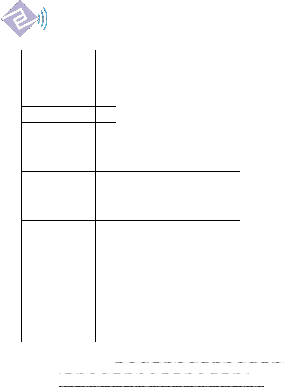
Pin
sequence
Pin
definition
I/O
描
述
PIN1
GND
Power ground
PIN2
GPIO0
I/O
General-purpose digital I/O (see the GPIO
part of the register description in
Chapter 13 of the HW3000 Datasheet for
details)
PIN3
GPIO1
I/O
PIN4
GPIO2
I/O
PIN5
VCC
Power supply 3.3V, power supply voltage
range 2.0V~3.6V
PIN6
SDO
O
SPI serial data output
PIN7
SDI
I
SPI serial data input
PIN8
SCK
I
SPI clock signal
PIN9
CSN
I
SPI chip select signal (active low)
PIN10
IRQ
O
Interrupt output pin (polarity can be
configured, the default low level is
effective)
PIN11
PDN
I
POWER DOWN mode enable input pin
(active high), and module hardware
reset pin
Power ground
PIN12
GND
Power ground
PIN14
ANT
RF antenna output, connect to 50 ohm
433 antenna
PIN15
GND
Power ground
Note: (If the user MCU pin number is really tight, GPIO0, GPIO1, GPIO2 can not
be connected; if the number of pins allows, GPIO0, GPIO1, GPIO2 are recommended
to receive one of them, but SDO, SDI, SCK, CSN, IRQ , PDN must be connected.)