
Specifications
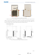
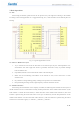
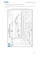
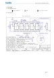
Table Of Contents

12 / 15
5 Production Guide
5.1 Production Guide
It is suggested processing SMT machine patch on the stamp tear sealing module, and finishing it
within 24 hours after unpacking. Otherwise, please vacuumize and package again, so as to prevent the
problem that the patch processing effect is poor due to damp. If there is a humidity indicator card in the
package, it is suggested judging if the module needs to be baked according to the indication of the
humidity card. The baking conditions are as follows:
Baking temperature: 125℃±5℃;
Alarm temperature: 130℃;
SMT patch processing can be carried out after the product is cooled to < 36℃ under natural
conditions.
If the unpacking time exceeds 3 months, whether the product got damp shall be paid special attention
to, because the gold immersion process of PCB may lead to the oxidation of the bonding pad when in
excess of 3 months, and such problems as pseudo soldering and solder skips.
In order to ensure the pass rate of reflow soldering, sampling 10% of products to carry out visual
inspection and take the AOI test in the first time of patch processing is suggested, so as to ensure the
reasonableness of furnace temperature control, device absorption mode, and placement method.
During the whole production process, the operators at all stations must wear antistatic gloves.
5.2 Requirements on Module Position on Bottom Plate
It is suggested that the thickness of liquid photosensitive solder resist at the module position on the
bottom plate be less than 0.02mm, to avoid excessive thickness causing the module unable to be effectively
contacted with the solder paste after being blocked up, thus affecting soldering quality.
In addition, please make sure not to put other devices within 2mm around the module position on the
interface board, so as to guarantee the maintenance of module.
5.3 Opening Design of Steel Mesh
If the thickness of steel mesh on the bottom plate is selected by comprehensively considering the
sealing type of the devices in the board in principle, pay close attention to the following requirements:
The bonding pad of module can be locally thickened to 0.15~0.20mm, to avoid missing solder.