Zigbee Module Data Sheet REX3T V1.1.
-1- Copyright The information contained in this document is the proprietary information of Zhejiang Raying loT Technology Co., Ltd. (hereinafter referred to as Rexense or the company). All rights reserved. Without the written permission of the company, the content of the document shall not be disclosed to the company's employees, agents, partners or any unauthorized parties in any form without authorization, copying or dissemination of this document is prohibited.
-2- Content 1. Product Introduction.............................................................................................................................................. - 3 1.1. Introduction......................................................................................................................................................... - 3 1.2. Application..........................................................................................................................................
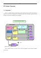
-3- 1. Product Introduction 1.1. Introduction With chip of TLSR825X, REX3T provides a complete 2.4GHz Zigbee system with high performance, low-consumption and low cost. This module conforms to Zigbee , integrating 32 byte MCU, 64KBS RAM,512KB Flash, 14byte ADC and 6-channel PWM, one QDEC and and sufficient GPIO. 1.2. Application REX3T conforms to Zigbee 3.0 Transparent communication: users can develop according to AT Command of REXENSE.
-4 512K Flash;64K RAM 14 GPIOs can be configured for various functional interfaces according to application GPIO External interrupts 14 bytes precision ADC channel USART Hardware flow control TWI interface SPI/I2C interface PWM output Hardware watchdog sampling
-5- 1.4. Product Advantage Package is small, which fits the small device well. Advanced link budget in the industry Outstanding battery longevity Big storage resource, good for client software application Powerful mesh network forming ability With development kit easy to use and cost-effective ISM band license free 1.5.
-6- 2. Product Overview 2.1. Overview REX3T is a ZigBee module of compact layout, higher sensitivity and lower power, and conforms to Zigbee 3.0 protocol, with outstanding RF characteristics, lower power consumption, powerful processor and big on-chip resource, and easy for user to integrate. XTAL (Crystal Frequency 24MHz) RISC 32bit MCU Power Management Data RAM 64kB Program Flash 512kB O-QPSK Modem SPI TWI Internal Oscillators RISC 32bit MCU MAC Accelerator Timers UART 2.
-7- 3. Technical Specification 3.1. Electrical Specification 3.1.1. Electrical Specification Table 3-1. Absolute Maximum Ratings Min Max Module input voltage(VCC) 1.8V 3.6V Pin voltage (except ADC pin) -0.3V VDD_PADS+0.3 ADC Pin voltage -3.3V 3.6V Parameter Data of maximum drive current of all I/Os 16 mA Maximum RF signal receiving density of chips +6 dBm Note: exceeding the absolute maximum ratings may damage module.
-8Parameter Test Conditions Range Unit Frequency range 2400~2483.5 Quantity of Channels 16 Channel No. 0B~1A Hex Channel spacing 5 MHz Transmitting power -9 to +10.0 dBm -100 dBm 50 Ω Receiving sensitivity ( 99% ) @IEEE802.15.4 250kpbs Rated Input / Output Impedance For unbalanced output MHz 3.1.4. Processor Characteristics Table 3-4.
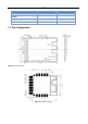
-9Parameter Physical size Weight *Working temperature Relative working Humidity Value 20.4*14.8*1.8mm <1g -40°C to +85°C(default) <95% 3.3. Pin Configuration Figure3-1.Layout Dimension Figure3-2.
- 10 - Figure 3-3. Pin Configuration Table 3-7. Pin Description Pin No of Module QFN32 Pin No of Packag e 1 23 PC2 I/O GPIO 2 15 PB5 I/O GPIO 3 6 PB1 I/O GPIO;TXD 4 23 PC3 I/O GPIO;RXD 5 9,18,33 3.
- 11 - Pin No of Module QFN32 Pin No of Packag e 13 31 PD2 I/O GPIO 14 28 PC0 I/O GPIO 15 29 PC1 IO GPIO 16 17 PB7 IO GPIO 17 5 SWS IO GPIO 18 7 GND I GND 19 8 RESET I RESET Pin signal 方向 Out put/ Inpu t Pin description
- 12 - 3.4. 天线规格 Antenna Specification REX3T has integrate different antennas, with details below: 3.4.1. PCB Antenna Figure 3-4. PCB Antenna With PCB antenna, there are points to be noted: 1. Avoid placing modules in a metal shell. 2. Keep metal object from the PCB antenna (at least 1cm above, 2.7cm plus recommend). 3. Do not keep module nearby the devices with electromagnetic radiation source, such as transformers.
- 13 - Components, traces, copper allowed No components around, or traces or copper at bottom. Preferred is hollow on top or at bottom of PCB antenna. Table 3-5.PCB Board Layout regarding to Positioning PCB Antenna of Module 3.5. Soldering Temperature for Module The max temperature for soldering module shall be within 237-245℃ in 20s. 3.6.
- 14 - 4.Zigbee transparent interface protocol 4.1.
- 15 - 4.2. 透传指令集 List of transparent command Table 4-3 CmdFunction cmdID General AT command set ParaLen Parameters Format Corresponding event Interval: Set Advertising Interval Set Advertising Data Enable/Disable Advertising 0xFF01 0x0002 <=0x0010 0xFF02 e.g. 0x0006 0xFF0A 0x0001 0xFF0C 0x0000 e.g. 0x0050 Advertising interval = 80* 0.625ms= 50ms Data set: e.g. Command 01 FF 02 00 50 Complete event 00 e.g. 02 FF 06 00 e.g.
- 16 - CmdFunction cmdID ParaLen Parameters Format Corresponding event Parameter 1: addrType Add White List Entry 0x00: Public Address 0xFF0F 0x0007 0x01: Random Address 0F FF 07 00 00 01 02 03 04 05 Command 06 Complete event Parameter 2: address e,g, 01 02 03 04 05 06 Delete White List 0xFF10 0x0007 Parameter 1: addrType e.g. 0x00: Public Address 10 FF 07 00 00 01 02 03 04 05 Command 06 Complete event 0x01: Random Address Parameter 2: address Entry e.g.
- 17 - Set connection parameters Parameters: 0xFF15 0x0008 u16 interval Min; e.g.
- 18 - CmdFunction cmdID ParaLen Parameters Format Corresponding event accepts minimum connection interval 0xA0*1.25ms=200ms u16 interval Max; e.g. 0x00A2 means current device accepts maximum connection interval 0xA2*1.25ms=202.5ms u16 connLatency; e.g. 0x0000 means current device expects new latency 0x00 u16 connTime out; e.g.
- 19 - fEnable Enable or Disable MAC Binding Function ‘0x01’: enable MAC binding 0xFF19 0x0001 function. After MAC binding is enabled, only the devices with MAC address in the MAC table can be connected with this module.
- 20 - CmdFunction cmdID ParaLen Parameters Format Corresponding event ‘0x00’: disable MAC binding function MacAddr Add device’s MAC address to MAC binding 0xFF1A 0x0006 table MAC address to be added into e.g. MAC binding table. 1A FF 06 00 Command Note: MAC table supports public B4 CE BF 01 Complete Event MAC address only. E7 60 e.g. B4 CE BF 01 E7 60 Delete a MAC item from MAC 0xFF1B 0x0006 binding table MacAddr e.g.
- 21 表 4-4 Event name Type Token General events ParaLen EventID Parameters Format corresponding to the command Rule: eventID = (cmdID Comman d Indicates status Synchronous 0xFF 0x03 & 0x03FF) | 0x0400 e,g, 0x0701 Complete (cmdID=0xFF01, event information Success: 0x00 Others: error e,g. FF 03 01 07 00 code, @ble_sts_t corresponding to the “Set Advertising Interval” command) Data received Asynchronous 0xFF Variable: data (indicates n+2 received data, n Eg.
- 22 - Connection parameter update Event Asynchronous 0xFF 0x02 0x078b NA FF 02 8b 07
- 23 - 4.3. How to interface 3T module Hardware interface protocol: Baud rate :115200 bps Data bits :8 Check bit :None Stop bit :1 Flow control :None 3T Module DC 3.3V VCC Host VCC GND GND GND UART_TX UART_RX UART_RX UART_TX Figure 4-1. Interface under normal condition 3T Module VCC GND DC 3.3V GND VCC GND UART_TX UART_RX UART_RX UART_TX GPIO GPIO Module wakeup Host Host wakeupModule Host GPIO GPIO Figure 4-2.
5. Ordering information Manufacturer REX=REXENSE Series 3=2.
- 25 - 6. Contact Us Zhejiang Raying IoT Technology Co., Ltd. Add:6F, Building No.4, No.6 Longzhou Road, Yuhang District,Hangzhou,311100, China Tel:+86-571-85395623 Fax:+86-571-87987620 Email: intl@rexense.com Web:www.rexense.
FCC Statement FCC standards: FCC CFR Title 47 Part 15 Subpart C Section 15.247 Integral PCB antenna with antenna gain 1.0dBi This device complies with part 15 of the FCC Rules. Operation is subject to the following two conditions: (1) This device may not cause harmful interference, and (2) this device must accept any interference received, including interference that may cause undesired operation.