cPCI-3920 Series 3U CompactPCI Blade with Intel® Core™2 Duo, Core™ Duo, Celeron® M Processor User’s Manual Manual Rev. 2.20 Revision Date: August 30, 2010 Part No: 50-15064-1020 Advance Technologies; Automate the World.
Revision History Revision Release Date Description of Change(s) 2.00 2008/07/07 Initial Release 2.10 2008/09/04 Update BIOS chapter 2.
cPCI-3920 Preface Copyright 2010 ADLINK Technology Inc. This document contains proprietary information protected by copyright. All rights are reserved. No part of this manual may be reproduced by any mechanical, electronic, or other means in any form without prior written permission of the manufacturer.
Using this Manual Audience and Scope The cPCI-3920 User’s Manual is intended for hardware technicians and systems operators with knowledge of installing, configuring and operating industrial grade CompactPCI modules. Manual Organization This manual is organized as follows: Chapter 1, Overview: Introduces the cPCI-3920 and package contents. Chapter 2, Specifications: Presents detailed specification information, power consumption, and mechanical layout.
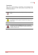
cPCI-3920 Conventions Take note of the following conventions used throughout this manual to make sure that users perform certain tasks and instructions properly. Additional information, aids, and tips that help users perform tasks. NOTE: CAUTION: WARNING: Preface Information to prevent minor physical injury, component damage, data loss, and/or program corruption when trying to complete a task.
This page intentionally left blank.
cPCI-3920 Table of Contents Revision History...................................................................... ii Preface .................................................................................... iii List of Tables.......................................................................... ix List of Figures ........................................................................ xi 1 Overview ............................................................................. 1 1.1 1.2 1.3 1.4 1.
5 Driver Installation.............................................................. 63 6 Watchdog Timer................................................................ 65 6.1 6.2 WDT Overview................................................................... 65 Using the Watchdog Timer in an Application ..................... 66 7 BIOS Setup Utility ............................................................. 71 7.1 7.2 7.3 7.4 7.5 7.6 7.7 7.8 Starting the BIOS ...........................................
cPCI-3920 List of Tables Table Table Table Table Table Table Table Table Table Table Table Table Table Table Table Table Table Table Table Table Table Table Table Table Table Table Table 2-1: 2-2: 2-3: 2-4: 2-5: 3-1: 3-2: 3-3: 3-4: 3-5: 3-6: 3-7: 3-8: 3-9: 3-10: 3-11: 3-12: 3-13: 3-14: 3-15: 3-16: 3-17: 3-18: 3-19: 3-20: 3-21: 3-22: List of Tables I/O Connectivity ...................................................... CompactPCI input voltage characteristics ..............
This page intentionally left blank.
cPCI-3920 List of Figures Figure 1-1: Figure 2-1: Figure 2-2: Figure 2-3: Figure 2-4: Figure 2-5: Figure 2-6: Figure 2-7: Figure 3-1: Figure 3-2: Figure 6-1: List of Figures cPCI-3920 Block Diagram ......................................... 3 cPCI-3920 Mechanical Dimensions......................... 15 cPCI-R3920 Mechanical Dimensions ...................... 16 cPCI-3920 Board Layout ......................................... 17 cPCI-3920A Assembly and Front Panel ..................
This page intentionally left blank.
cPCI-3920 1 Overview 1.1 Introduction The cPCI-3920 is a highly integrated 3U CompactPCI SBC in single slot (4HP) or dual slot (8HP) width form factor. It has been designed to support Intel® lower power Core™ 2 Duo, Core™ Duo and Celeron® M processors in FC-BGA package with a range of 1.0GHz to 1.5GHz at FSB 533MHz to 667MHz. They deliver optimized power-efficient computing and outstanding dual core performance with lower power consumption.
1.2 Features 2 X 3U CompactPCI SBC in 4HP or 8HP width form factor X Low power Intel Core 2 Duo 1.5GHz, Core™ Duo 1.2GHz, Celeron® M 1.0GHz processors X Intel® 3100 chipset (Memory and I/O Hub integrated chip) X Single channel DDR2 registered and ECC memory at 400MHz X Two PCI-Express Gigabit Ethernet ports in the front or RTM X Support USB 2.0 NAND flash module, up to 8GB X Supports one 2.
cPCI-3920 1.
1.4 Product List Products included in the cPCI-3920 Series include: SBC X cPCI-3920A: single-slot (4HP) width 3U CompactPCI featuring Intel LV Core 2 Duo 1.5GHz, Core Duo 1.2GHz or ULV Celeron 1.0GHz processors; 512MB, 1GB or 2GB onboard memory; optional USB flash disk module X cPCI-3920B: dual-slot(8HP) width 3U CompactPCI featuring Intel LV Core 2 Duo 1.5GHz, Core Duo 1.2GHz or ULV Celeron 1.0GHz processors; 512MB, 1GB or 2GB onboard memory; optional USB flash disk module and 2.
cPCI-3920 1.5 Package Contents The cPCI-3920 is packaged with the following components. If any of the items on the contents list are missing or damaged, retain the shipping carton and packing material and contact the dealer for inspection. Please obtain authorization before returning any product to ADLINK. The packing contents of the cPCI-3920 Series are non-standard configurations and may vary depending on customer requests.
This page intentionally left blank.
cPCI-3920 2 Specifications 2.1 CPU, memory, and chipset uFC-BGA Intel® Core™ 2 Duo LV (L7400) 1.5 GHz, FSB 667MHz, 4 MB L2 cache Processor uFC-BGA Intel Intel® Core™ Duo ULV (U2500) 1.2 GHz, FSB 533MHz, 2 MB L2 cache uFC-BGA Intel Intel® Celeron® M ULV (423) 1.06 GHz, FSB 533MHz, 1 MB L2 cache Chipset Intel® 3100 chipset Memory Single channel soldered onboard registered ECC DDR2 SDRAM at 400MHz up to 2GB 2.2 Interfaces CompactPCI Standard PICMG® 2.0 R3.0 PICMG® 2.1 R2.
4x serial ports Serial Port Two DB-9 ports on the front panel, one RS-232 and one RS-232/422/485/485+ (8HP only) Two ports are routed to RTM with one DB-9 port on rear panel and one pin header onboard 4x Serial ATA channels: Serial ATA One SATA connector onboard, 2.5” HDD space reserved (8HP only) Three channels are routed to RTM with pin headers onboard cPCI-3920 main board 1x USB 2.
cPCI-3920 2.3 Software BIOS AMI 16Mbit FWH Microsoft® Windows® XP Professional Microsoft® Windows® Server 2003 Supported OS Microsoft® Windows® Vista Enterprise, 32-bit version RedHat Fedora Core 8 Contact ADLINK for other OS availability 2.4 Mechanical Form factor cPCI-3920: 3U 4HP/8HP CompactPCI cPCI-R3920(T): 3U 4HP CompactPCI cPCI-3920: 100mmx 160mm (LxW) Dimensions cPCI-R3920: 100mm x 50mm (LxW) cPCI-R3920T: 100mmx 80mm (LxW) 2.
2.
cPCI-3920 2.7 Power Requirements In order to guarantee a stable functionality of the system, it is recommended to provide more power than the system requires. An industrial power supply unit should be able to provide at least twice as much power as the entire system requires. An ATX power supply unit should be able to provide at least three times as much power as the entire system requires. The tolerance of the voltage lines described in the CompactPCI specification (PICMG 2.0 R3.0) is +5%/ -3% for 5, 3.
Power Consumption The following tables provide information on the power consumption of cPCI-3920. Processor: Intel® Core™ 2 Duo LV (L7400) 1.5GHz, FSB 667MHz, 4MB L2 cache Function Memory SATA Hard Drive Backplane Power Supply DOS Power requirement Current (A) Watts (W) Configuration DDR2 400 1GB External 3.5”HDD ADLINK cBP-3208R Rev.B2 ZIPPY HG2-6350P 350W +3.3V 1.53 5.05 +5V 4.41 22.05 Total Linux, Idle Power requirement Current (A) Watts (W) +3.3V 1.63 5.38 +5V 3.53 17.
cPCI-3920 Processor: Intel® Core™ Duo (U2500) 1.2GHz, FSB 533MHz, 2MB L2 cache Function Memory SATA Hard Drive Backplane Power Supply DOS Power requirement Current (A) Watts (W) Configuration DDR2 400 1GB External 3.5”HDD ADLINK cBP-3208R Rev.B2 ZIPPY HG2-6350P 350W +3.3V 1.54 5.08 +5V 3.50 17.50 Total Linux, Idle Power requirement Current (A) Watts (W) +3.3V 1.64 5.41 +5V 3.30 16.50 Total Windows® XP, Idle Power requirement +3.3V Current (A) 1.68 Watts (W) 5.38 +5V 3.71 18.
Processor: Intel® Celeron M LV(423) 1.07GHz, FSB 533MHz, 1MB L2 cache Function Memory SATA Hard Drive Backplane Power Supply DOS Power requirement Current (A) Watts (W) Configuration DDR2 400 1GB External 3.5”HDD ADLINK cBP-3208R Rev.B2 ZIPPY HG2-6350P 350W +3.3V 1.51 4.98 +5V 3.27 16.35 Total Linux, Idle Power requirement Current (A) Watts (W) +3.3V 1.60 5.28 +5V 3.12 15.60 Total Windows® XP, Idle Power requirement +3.3V Current (A) 1.59 Watts (W) 5.25 +5V 3.36 16.
cPCI-3920 2.
cPCI-R3920 cPCI-R3920T Figure 2-2: cPCI-R3920 Mechanical Dimensions 16 Specifications
cPCI-3920 2.
cPCI-3920A Assembly Outline Thermal Module USB flash disk (optional) Battery cPCI-3920A Front Panel Speed ACT Figure 2-4: cPCI-3920A Assembly and Front Panel Reset Button X RST Temperature LED X Hot (red): CPU Overtemperature Status, connected to the CPU signal PROCHOT Status LEDs X WDT (yellow): Watchdog Status X PWR (green): Power Supply Status Gigabit Ethernet LEDs 18 X SPEED ON (green): 1000Mbps X SPEED OFF: 10Mbps or 100Mbps X ACT (yellow): Ethernet Link Activity Specifications
cPCI-3920 DB-3920L2 Daughter Board Components Layout The DB-3920L2 Daughter Board extends the cPCI-3920 from 4HP (cPCI-3920A) to 8HP (cPCI-3920B) version. This additional capability opens up the broadest range of expansion possibilities. The DB-3920L2 module has been designed to include two COM ports, a PS/2 keyboard and mouse port, two USB 2.0 interfaces and a 2.5” SATA hard disk interface.
cPCI-3920B Assembly Outline 2.
cPCI-3920 cPCI-R3920(T) Board Layout The cPCI-3920 Series offer two version rear transition modules with the same functionality but different dimensions.
This page intentionally left blank.
cPCI-3920 3 Functional Description The following sections describe the cPCI-3920 main functions and board interfaces. 3.1 CPU, Memory and Chipset CPU: Intel® Core™ Duo and Intel® Core™2 Duo The cPCI-3920 supports the latest Intel® Core™ Duo and Intel® Core™2 Duo processor family up to speeds of 1.5 GHz with up to 667 MHz FSB. The Intel® Core™ Duo consists of two cores and up to 2 MB L2 cache shared by both cores.
The following list sets out some of the key features of the Intel® Core™ Duo and the Intel® Core™2 Duo processors: X Two mobile execution cores in one single processor X Support of Intel’s Virtualization Technology (Vanderpool) X Support of Intel Architecture with Dynamic Execution X Outstanding dual-core performance with low power consumption X On die, primary 32 KB instruction cache and 32KB writeback data cache X On die, L1 and L2 cache with Advanced Transfer Cache Architecture Z Intel® Core™
cPCI-3920 agement that reduce the number of micro-ops handled by the processor. X On-die, primary 32-kB instruction cache and 32-kB, writeback, data cache X On-die, 1 MB second level cache with Advanced Transfer Cache architecture X Advanced branch prediction and data prefetch logic X Streaming SIMD extensions 2 (SSE2) that enables breakthrough levels of performance in multimedia applications including 3D graphics, video decoding/encoding, and speech recognition.
Memory The cPCI-3920 supports a single soldered channel DDR2 memory with Error Checking and Correcting (ECC) running at 400 MHz The available memory module configuration is 1 GB. 2 GB available on request, please contact your ADLINK representative. NOTE: Memory configuration changes can only be performed at the factory. Failure to comply with the above may result in damage to your board or improper operation.
cPCI-3920 PCI Express The Intel 3100 Chipset provides one configurable x8 PCI Express interface with a maximum theoretical bandwidth of 4 GByte/s. The x8 PCI Express interface may alternatively be configured as two independent x4 PCI Express interfaces with a maximum theoretical bandwidth of 2 GBytes/s each.
X System TCO Reduction Circuits X SMBus X Watchdog Timers X PCI 2.3 Interface X Two fully functional serial ports X 38 General Purpose I/Os (GPIO) IMCH The Intel® 3100 Chipset provides an integrated memory controller for direct-connection to one channel of DDR2-400 (unstacked) registered memory devices with ECC. Peak theoretical memory data bandwidth using DDR2-400 is 3.2 GByte/s Volari™ Z11 Graphics Controller Volari™ Z11 GPU is the extreme programmable GPU of the XGI 2D GPU family.
cPCI-3920 X Z Supports DDR-II SDRAM memory Z 32 MB memory configuration Z Supports VGA BIOS auto memory size detection High Performance Flat Panel Display Interface Z X X X High Integration Z Built-in CRT FIFO to support ultra high resolution graphics modes and reduce CPU wait-state Z Built-in programmable 24-bit true-color RAMDAC with 230 MHz pixel clock Resolution, Color & Frame Rate Z Supports 230 MHz pixel clock Z Supports VESA standard super high resolution graphics modes 4:3 resolut
3.2 Peripherals The following standard peripherals are available on the cPCI-3920 board: Timer The cPCI-3920 is equipped with the following timers: Real-Time Clock The IICH contains real-time clock with 256-byte of batterybacked RAM. The real-time clock performs timekeeping functions and includes 256 bytes of general purpose battery-backed CMOS RAM. Features include an alarm function, programmable periodic interrupt and a 100-year calendar.
cPCI-3920 Battery The cPCI-3920 is provided with a 3.0 V “coin cell” lithium battery for the RTC. To replace the battery, proceed as follows: X Turn off power X Remove the battery X Place the new battery in the socket. X Make sure that you insert the battery the right way round. The plus pole must be on the top! The lithium battery must be replaced with an identical battery or a battery type recommended by the manufacturer. Suitable batteries include the Varta CR2025 and Panasonic BR2020.
Reset A reset will be generated by the following conditions: X Pressing the front panel reset button X Watchdog overflow X CompactPCI backplane PRST# input (CompactPCI connector J2, pin C17) SMBus Devices The cPCI-3920 provides a System Management Bus (SMBus) for access to several system monitoring and configuration functions. The SMBus consists of a two-wire I2C bus interface. The following table describes the function and address of every onboard SMBus device.
cPCI-3920 FWH Flash Memory For simple BIOS updating a standard onboard 16 Mbit Firmware Hub device is used. The FWH stores both the system BIOS and graphics BIOS. It can be updated as new versions of the BIOS become available. LED Functions There are three LEDs on the front panel, below table shows the function of LEDs. Name HOT Color Status Function description BLINK CPU reaches or exceeds max. operating temperature OFF CPU below max.
3.3 Board Interfaces USB Interfaces The cPCI-3920 supports six USB 2.0 ports: X one front I/O X two front I/O on DB-3920L2 module X one onboard to connect a Flash disk X two on the Rear I/O module. On the USB 2.0 front panel port, USB cable with up to 5 meters in length can be used. On the USB 2.0 Rear I/O ports, it is strongly recommended to use a cable below 3 meters in length for USB 2.0 devices. The USB 2.0 ports are high-speed, full-speed, and low-speed capable. Hi-speed USB 2.
cPCI-3920 Onboard USB Pin Header (CN5) The onboard USB device (CN5 pin header, 2.54mm pitch) is used to connect a USB Flash Disk.
USB Flash Disk Mechanical Layout X Maximum space reserved for USB flash disk is 50mm x 30mm (LxW) X The distance between the centers of connector and screw hole is 27.3mm~27.9mm X Maximum allowable connector height is 9.
cPCI-3920 Graphics Controller The Volari™ Z11 graphics controller incorporates a powerful 64-bit graphics engine to enhance the performance of 2D operations. The capabilities of the graphics engine include, but are not limited to BitBlt, Color Expansion, Enhanced Color Expansion, Line Drawing, Transparent BitBlt, and Rectangle Fill.
interface at 250MHz. It can support up to a 1GB/s bandwidth, with a 16-bit DDRII SDRAM interface. A DRAM capacity of 32MB is currently supported on cPCI3920 boards. VGA Analog Interface and Connector (CN3) The 15-pin female connector CN3 is used to connect a VGA analog monitor to the cPCI-3920 board. Signal Name Pin # Pin # Signal Name Red 1 2 Green Blue 3 4 N.C. GND 5 6 GND GND 7 8 GND +5V. 9 10 GND N.C.
cPCI-3920 Gigabit Connector RJ-45 Pin Definitions (CN7/CN8) The CN7/CN8 connector supplies the 10Base-T, 100BaseTX and 1000Base-T interfaces to the Ethernet controller.
remains off, a valid link has not been established due to a missing or a fault connection. Status Speed LED Act LED Network link is not established OFF OFF 10/100 Mbps 1000 Mbps Link OFF ON Active OFF Blink Link ON ON Active ON Blink Table 3-8: Ethernet LED Status Definitions Board-to-Board Connector The 60-pin female Board-to-Board Connector (CN4) connects the main board to the DB-3920L2 daughter board, allowing I/O expansion and HDD connectivity for the cPCI-3920B 8HP version.
cPCI-3920 CN4 Pin Assignment SIGNAL GND USB3-DUSB3-D+ GND USB2_DUSB2_D+ GND SATA0_RXSATA0_RX+ GND SATA0_TX+ SATA0_TXGND USB3_PWR USB2_PWR LPC_LDRQ0# A20GATE SERIRQ# KBD_RST# CPU_PWRGD XDP_DBRESET# TDI TMS TRST# TCK TDO +1.05V +1.
Keyboard/ Mouse Interface The keyboard controller is located on the cPCI-3920B and is 8042 software compatible. The PC/AT standard keyboard/mouse connector is a PS/2-type 6pin shielded Mini-DIN connector. A Y-cable to connect a mouse device and/or a keyboard to the PS/2 connector is included in the package of cPCI-3920B.
cPCI-3920 Universal Serial Ports Two PC-compatible serial RS-232, 9-pin D-Sub ports are available and fully compatible with the 16C550 controller. These port includes a complete set of handshaking and modem control signals. Data transfer rates up to 115.2 kB/s are supported. The COM3 interface is routed to the connector CN1.
COM4 Mode Switch Settings RS232 Full Modem RS422 Half Duplex RS485 Half Duplex RS485+ Half Duplex Location SW1 SW2 SW3 SW4 1 ON ON OFF ON 2 OFF OFF OFF OFF 3 ON ON OFF OFF 4 OFF OFF OFF OFF 1 OFF OFF ON OFF 2 ON ON ON ON 3 OFF OFF OFF OFF 4 ON ON OFF OFF 1 OFF OFF ON OFF 2 ON ON ON OFF 3 OFF OFF OFF ON 4 ON ON OFF OFF 1 OFF OFF OFF OFF 2 ON ON OFF OFF 3 OFF OFF ON OFF 4 ON ON ON ON Table 3-13: COM4 Mode Switch Settings
cPCI-3920 Serial ATA Interfaces The cPCI-3920 provides up to four SATA interfaces. Three SATA ports, SATA1, SATA2 and SATA3, can be used only on the Rear Transition Module I/O interface. All SATA ports can be used simultaneously. SATA Port Connector Usage SATA0 CN3-2 on the cPCI-3920B Onboard 2.5” DATA HDD drive mounted on CPCI-3920B SATA1 CN5-R on the cPCI-R3920(T) External SATA HDD drives, e.g. 2.5” or 3.5” SATA HDDs SATA2 CN4-R on the cPCI-R3920(T) External SATA HDD drives, e.g. 2.5” or 3.
SATA0 Connector, CN3-2 PIN SIGNAL FUNCTION Signal Segment Key I/O S1 GND Ground signal -- S2 SATA_TX2+ Differential Transmit+ O S3 SATA_TX2- Differential Transmit- O S4 GND Ground signal -- S5 SATA_RX2- Differential Receive- I S6 SATA_RX2+ Differential Receive+ I S7 GND Ground signal -- Signal Segment "L" Central Connector Polarizer Power Segment "L" P1 NC (3.3V) Not connected -- P2 NC (3.3V) Not connected -- P3 NC (3.
cPCI-3920 CompactPCI Bus Interfaces The complete CompactPCI connector configuration comprises two connectors named J1 and J2. Their function is as follows: X J1: 32-bit CompactPCI interface with PCI bus signals, arbitration, clock and power X J2: has optional Rear I/O interface functionality or 64-bit termination The board is capable of driving up to seven CompactPCI slots, with individual arbitration and clock signals.
CompactPCI J1 Pin Assignment Pin Z A B C D E F 25 GND +5V REQ64# ENUM# +3.3V +5V GND 24 GND AD[1] +5V V(I/O) AD[0] ACK64# GND 23 GND +3.3V AD[4] AD[3] +5V AD[2] GND 22 GND AD[7] GND +3.3V AD[6] AD[5] GND 21 GND +3.3V AD[9] AD[8] M66EN(2) C/ BE[0]# GND 20 GND AD[12] GND V(I/O) AD[11] AD[10] GND 19 GND +3.3V AD[15] AD[14] GND AD[13] GND 18 GND SERR# GND +3.3V PAR C/ BE[1]# GND 17 GND +3.3V N.C. N.C.
cPCI-3920 CompactPCI J2 Pin Assignment The cPCI-3920 board provides Rear I/O connectivity for special compact systems. Some standard PC interfaces are implemented and assigned to the front panel and to the rear connector J2. When the Rear I/O module is used, the signals of some of the main board/front panel connectors are routed to the Rear I/O module interface. Thus the Rear I/O module makes it much easier to remove the CPU in the rack as there is practically no cabling on the CPU board.
Legend for J2 Pin Assignment USBx USB interface and power ETHx Gigabit Ethernet port SATAx Serial ATA port COMx COM port GPIO x GPIO PEX_RX0Lx PEX_TX0Lx Pin Z A B 1 x4 or 4 x1 PCI-Express C D E F 22 N.C GA[4] GA[3] GA[2] GA[1] GA[0] GND 21 N.C CLK[6] GND COM1_RXD COM2_RXD GPIO7 GND 20 N.C CLK[5] GND COM1_TXD COM2_TXD GPIO6 GND 19 N.C GND/CLK100+ GND/CLK100+ SMB_SDA SMB_SCL SMB_ALERT GND 18 N.C SATA3_TX+ SATA3_TX- GND SATA3_RX+ SATA3_RX- GND 17 N.
cPCI-3920 3.4 Board Interfaces on RTM There are two identical USB interfaces on the CPCI-R3920(T) RTM, each with a maximum transfer rate of 480 Mb!s provided for connecting USB devices. One USB peripheral may be connected to each port. To connect more USB devices than there are available ports, an external hub is required.
Gigabit Connector RJ-45 Pin Definitions (CN6-R) The CN7/CN8 connector supplies the 10Base-T, 100BaseTX and 1000Base-T interfaces to the Ethernet controller.
cPCI-3920 COM1 DB-9 Serial Port Connector (CN3-R) Pin # RS-232 1 not used 2 RXD, Receive data 3 TXD, Transmit data 4 not used 5 GND, Ground 6 not used 7 not used 8 not used 9 not used Table 3-19: COM1 Serial Port Connector Pin Definition COM2 Onboard Serial Port Connector (CN1-R) Pin # RS-232 1 not used 2 not used 3 RXD, Receive data 4 not used 5 TXD, Transmit data 6 not used 7 not used 8 not used 9 GND, Ground 10 NC Table 3-20: COM2 Serial Port Connector Pin Defi
Serial ATA Interfaces - SATA1-3 The onboard Serial ATA connectors CN2-R, CN4-R and CN5-R allow the connection of standard HDDs and other Serial ATA devices to the cPCI-3920 Rear Transition Module. The following figure and table provide pinout information for the SATA connectors CN2-R, CN4-R and CN5-R.
cPCI-3920 Rear I/O Interfaces on CompactPCI Connector rJ2 The cPCI-3920 Rear Transition Module conducts a wide range of I/O signals through the Rear I/O connector rJ2. To support the Rear I/O feature a special backplane is necessary. Do not plug a Rear I/O configured board in a non-system slot Rear I/O backplane. Failure to comply with the above may result in damage to your board.
CompactPCI rJ2 Pin Assignment Legend for rJ2 Pin Assignment Pin Z USBx USB interface and power ETHx Gigabit Ethernet port SATAx Serial ATA port COMx COM port A B C D E F 22 N.C. GA[4] GA[3] GA[2] GA[1] GA[0] GND 21 N.C. CLK[6] GND COM1_RXD COM2_RXD N.C. GND 20 N.C. CLK[5] GND COM1_TXD COM2_TXD N.C. GND 19 N.C. GND/CLK100 GND/CLK100 SMB_SDA SMB_SCL SMB_ALERT GND 18 N.C. SATA3_TX+ SATA3_TX- GND SATA3_RX+ SATA3_RX- GND 17 N.C.
cPCI-3920 4 Getting Started The cPCI-3920 has been designed for easy installation. However, the following standard precautions, installation procedures, and general information must be observed to ensure proper installation and to preclude damage to the board, other system components, or injury to personnel. 4.1 Safety Requirements The following safety precautions must be observed when installing or operating the cPCI-3920.
4.2 Installing the USB Flash Disk The cPCI-3920 supports an onboard USB Flash Disk module via the CN5 pin header. To install a USB Flash Disk, follow the procedure below. 1. Secure the standoff to the underside of the module with the screw provided. 2. Align the module with the CN5 pin header and mounting hole as shown. 3. Insert the module onto the pin header and secure with the screw provided from the back side of the cPCI-3290.
cPCI-3920 4.3 Installing the Hard Disk Drive (cPCI-3290B only) The cPCI-3920B supports a slim-type 2.5” SATA HDD. If the cPCI3920 comes with a pre-installed HDD, proceed to the next section. To install the hard disk drive: 1. Place the HDD into the bracket as shown. 2. Insert the the HDD into the CN3-2 SATA signal/power connector. CN3-2 3. Tighten all four bracket screws to secure the HDD in place.
4.4 Installing the cPCI-3920 to the Chassis To install the cPCI-3920 module to a CompactPCI chassis: 1. Refer to the chassis documentation before installing the cPCI-3920. 2. Turn off the power in both chassis front and rear. 3. Assign a system slot for the board. Make sure you assign the correct slot. 4. Remove the panel cover of the slot you have selected. 5. Remove the black plastic caps securing the mounting screws to the front panel. 6.
cPCI-3920 4.5 RTM (cPCI-R3920) Installation Follow the typical cPCI board installation and removal procedures for the RTM. However, be careful when when inserting or removing RTMs to the chassis as these are shorter than front boards. Refer to previous sections when connecting or installing peripherals to the RTM. Make sure that the RTMs you are installing are compatible with the cPCI-3920 Series. NOTE: You must install the correct RTM to enable some functionalities (I/O interfaces) on the rear panel.
This page intentionally left blank.
cPCI-3920 5 Driver Installation The cPCI-3920 drivers are available from the ADLINK All-In-One CD at X:\cPCI\cPCI-3920\, or from the ADLINK website (http://www.adlinktech.com). The following describes the driver installation procedures for Windows® 2000, Windows® XP or Windows® Server 2003: 1. Install the Windows operating system before installing any driver. Most standard I/O device drivers are installed during Windows installation. 2. Install the chipset driver by running the program ...
This page intentionally left blank.
cPCI-3920 6 Watchdog Timer 6.1 WDT Overview This section explains the operation of the cPCI-3920’s Watchdog Timer (WDT). The primary function of the WDT is to monitor the cPCI-3920 operation and to reset the system if a software application fails to function as programmed.
the internal IO to control the WDT and retrieve its status. The basic functions of the WDT include: X Setting the watchdog timeout interval X Starting the timer countdown X Selecting 1 step or 2 step WDT X Enabling or disabling WDT X Reloading the timeout value to keep the watchdog from timing out X Setting the range of the timeout period from 1 µs to 1 second, or from 1 ms to 1050 seconds When the watchdog times out, it will send a RESET signal to the system. 6.
cPCI-3920 void write_config_data_byte(unsigned char,unsigned char); unsigned char read_config_data_byte(unsigned char); unsigned int read_wdt_io_base(); /* access wdt I/O registers routines */ void write_preload_val2_reg(unsigned long int); void clear_preload_val1_reg(); void unlocking_reg(); /* Global parameter */ unsigned int wdt_io_base; void main(void) { // unsigned int wdt_io_base; unsigned long int time_out_val=0; wdt_io_base=read_wdt_io_base(); printf("Intel 3100 Chipset Watch-Dog Timer test utility.
outportb(wdt_io_base+0x18,2);//watchdog timer enable!! printf("\nPlease waiting for Watch-Dog Timer time-out!!"); } /************************************/ unsigned int read_wdt_io_base() { unsigned char_wdt_io_base[2]; int *p_wdt_io_base; p_wdt_io_base=&_wdt_io_base; enter_config_mode(); write_config_data_byte(0x07,6);//select logic 6 - WDT _wdt_io_base[1]=read_config_data_byte(0x60) ; _wdt_io_base[0]=read_config_data_byte(0x61) ; exit_config_mode(); return (*p_wdt_io_base); } /****************************
cPCI-3920 outportb(0xeb,00); //io delay outportb(config_port_index,0x08); } /************************************/ unsigned char read_config_data_byte(unsigned char _index) { unsigned char r_data; outportb(config_port_index,_index); outportb(0xeb,00); //io delay r_data=inportb(config_port_data); return(r_data); } /************************************/ void write_config_data_byte(unsigned char _index,unsigned char _data) { outportb(config_port_index,_index); outportb(0xeb,00); //io delay outportb(config_por
// unlocking_reg(); outportb(wdt_io_base+5,*p_data); p_data++; printf("%x\n",*p_data); unlocking_reg(); outportb(wdt_io_base+6,*p_data); } /************************************/ void clear_preload_val1_reg() { unlocking_reg(); outportb(wdt_io_base,0x00); unlocking_reg(); outportb(wdt_io_base+1,0x00); unlocking_reg(); outportb(wdt_io_base+2,0x00); } /************************************/ void unlocking_reg() { outportb(wdt_io_base+12,0x80); outportb(0xeb,00); //io delay outportb(wdt_io_base+12,0x86); 70
cPCI-3920 7 BIOS Setup Utility The following chapter describes basic navigation for the AMIBIOS®8 BIOS setup utility. 7.1 Starting the BIOS To enter the setup screen, follow these steps: 1. Power on the motherboard 2. Press the < Delete > key on your keyboard when you see the following text prompt: < Press DEL to run Setup > 3. After you press the < Delete > key, the main BIOS setup menu displays. You can access the other setup screens from the main BIOS setup menu, such as Chipset and Power menus.
Setup Menu The main BIOS setup menu is the first screen that you can navigate. Each main BIOS setup menu option is described in this user’s guide. The Main BIOS setup menu screen has two main frames. The left frame displays all the options that can be configured. “Grayed” options cannot be configured, “Blue” options can be. The right frame displays the key legend. Above the key legend is an area reserved for a text message. When an option is selected in the left frame, it is highlighted in white.
cPCI-3920 These keys include < F1 >, < F10 >, < Enter >, < ESC >, < Arrow > keys, and so on. . There is a hot key legend located in the right frame on most setup screens. NOTE: The < F8 > key on your keyboard is the Fail-Safe key. It is not displayed on the key legend by default. To set the Fail-Safe settings of the BIOS, press the < F8 > key on your keyboard. It is located on the upper row of a standard 101 keyboard.
F10 The < F10 > key allows you to save any changes you have made and exit Setup. Press the < F10 > key to save your changes. The following screen will appear: Press the < Enter > key to save the configuration and exit. You can also use the < Arrow > key to select Cancel and then press the < Enter > key to abort this function and return to the previous screen. ESC The < Esc > key allows you to discard any changes you have made and exit the Setup.
cPCI-3920 7.2 Main Setup When you first enter the Setup Utility, you will enter the Main setup screen. You can always return to the Main setup screen by selecting the Main tab. The Main BIOS Setup screen is shown below. System Time/System Date Use this option to change the system time and date. Highlight System Time or System Date using the < Arrow > keys. Enter new values using the keyboard. Press the < Tab > key or the < Arrow > keys to move between fields. The date must be entered in MM/ DD/YY format.
Input UUID Use this function to set a unique Universally Unique Identifier (UUID) for the system. UUID Byte 0-7 This field sets bytes 0-7 of the UUID. UUID Byte 8-F This field sets bytes 8-F of the UUID.
cPCI-3920 7.3 Advanced BIOS Setup Select the Advanced tab from the setup screen to enter the Advanced BIOS Setup screen. You can select any of the items in the left frame of the screen to go to the sub menu for that item. You can display an Advanced BIOS Setup option by highlighting it using the < Arrow > keys. The Advanced BIOS Setup screen is shown below. The sub menus are described on the following pages. CPU Configuration You can use this screen to select options for the CPU Configuration Settings.
Intel® Core™2 Duo L7400 Hardware Prefetcher The processor has a hardware prefetcher that automatically analyzes its requirements and prefetches data and instructions from the memory into the Level 2 cache that are likely to be required in the near future. This reduces the latency associated with memory reads. When Enabled, the processor's hardware prefetcher will be enabled and allowed to automatically prefetch data and code for the processor.
cPCI-3920 This reduces cache latency by making the next cache line immediately available if the processor requires it as well. When Enabled, the processor will retrieve the currently requested cache line, as well as the subsequent cache line. When Disabled, the processor will only retrieve the currently requested cache line.
CPU Frequency on XP/Linux This option is used to manually set the CPU frequency on XP and Linux operating systems. The following options are available: 1500MHz, 1333MHz, 1166MHz, and 1000MHz. Intel® Core™ Duo U2500 Intel® Virtualization Technology This is used to enable or disable the Intel® Virtualization Technology (IVT) extension, which is also known by the development code name of Vanderpool. It allows multiple operating systems to run simultaneously on the same system.
cPCI-3920 Intel® SpeedStep™ Techology This allows you to enable or disable Intel® SpeedStep™ Technology.
IDE Configuration You can use this screen to select options for the IDE Configuration Settings. Use the up and down < Arrow > keys to select an item. Use the < + > and < - > keys to change the value of the selected option. A description of the selected item appears on the right side of the screen. The settings are described on the following pages. An example of the IDE Configuration screen is shown below.
cPCI-3920 Primary IDE Master, Primary IDE Slave, Secondary IDE Master, Secondary IDE Slave Select one of the hard disk drives to configure it. Press < Enter > to access its sub menu. Hard Disk Write Protect This will be affective only if device is accessed through BIOS. The settings are Enabled and Disabled. IDE Detect Time Out (Sec) Select the time out value for detecting ATA/ATAPI devices. The settings are 0 sec, 5 sec, 10 sec, 15 sec, 20 sec, 25sec, 30 sec, and 35 sec.
Hardware Health Configuration This option displays the current status of all of the monitored hardware devices / components such as voltages and temperatures.
cPCI-3920 Remote Access Configuration Remote Access Configuration provides the settings to allow remote access by another computer to get POST messages and send commands through serial port access. Remote Access Select this option to Enabled or Disabled the BIOS remote access feature. Serial Port Number Select the serial port you want to use for the remote access interface. You can set the value for this option to either COM1 or COM2. The Base Address and IRQ of the selected serial port is displayed.
Serial Port Mode Select the baud rate you want the serial port to use for console redirection. The options are 115200 8,n,1; 57600 8,n,1; 19200 8,n,1; and 09600 8,n,1. Flow Control Set this option to select Flow Control for console redirection. The settings for this value are None, Hardware, or Software. Terminal Type This option is used to select either VT100/VT-UTF8 or ANSI terminal type. The settings for this value are ANSI, VT100, or VT-UTF8.
cPCI-3920 USB Configuration You can use this screen to select options for the USB Configuration. Use the up and down < Arrow > keys to select an item. Use the < + > and < - > keys to change the value of the selected option. The settings are described on the following pages. The screen is shown below. Legacy USB Support Legacy USB Support refers to USB mouse and keyboard support.
Disabled Set this value to prevent the use of any USB device in DOS or during system boot. Enabled Set this value to allow the use of USB devices during boot and while using DOS. Auto This option auto detects USB Keyboards or Mice and if found, allows them to be utilized during boot and while using DOS. Port 64/60 Emulation It uses USB to receive the IO port 64/60 trap to emulate the legacy keyboard controller. USB 2.0 Controller Mode The USB 2.0 Controller Mode configures the data rate of the USB port.
cPCI-3920 7.4 PCI/PnP Setup Select the PCI/PnP tab from the setup screen to enter the Plug and Play BIOS Setup screen. You can display a Plug and Play BIOS Setup option by highlighting it using the < Arrow > keys. The Plug and Play BIOS Setup screen is shown below. IRQ Set this value to allow the IRQ settings to be modified. Available – This setting allows the specified IRQ to be used by a PCI/PnP device. Reserved – This setting allows the specified IRQ to be used by a legacy ISA device.
device. Reserved – This setting allows the specified DMA to be used by a legacy ISA device. 7.5 Boot Setup Select the Boot tab from the setup screen to enter the Boot BIOS Setup screen. You can select any of the items in the left frame of the screen, such as Boot Device Priority, to go to the sub menu for that item. You can display a Boot BIOS Setup option by highlighting it using the < Arrow > keys.
cPCI-3920 Boot Setting Configuration Use this screen to select options for the Boot Settings Configuration. Use the up and down keys to select an item. Use the and keys to change the value of the selected option. The settings are described on the following pages. The screen is shown below. Quick Boot Disabled – Set this value to allow the BIOS to perform all POST tests. Enabled – Set this value to allow the BIOS to skip certain POST tests to boot faster.
Boot Device Priority Boot Devices Priority This specifies the boot sequence from the available devices. The 1st Boot Device is primary device.
cPCI-3920 Removable Drives Removable Drives This specifies the Boot Device Priority sequence from available Removable Drives. Disabled – Set this menu to allow the BIOS to remove device on Boot Device Priority.
7.6 Security Setup Password Support Two Levels of Password Protection Provides both a Supervisor and a User password. If you use both passwords, the Supervisor password must be set first. The system can be configured so that all users must enter a password every time the system boots or when Setup is executed, using either or either the Supervisor password or User password. The Supervisor and User passwords activate two different levels of password security.
cPCI-3920 Remember the Password Keep a record of the new password when the password is changed. If you forget the password, you must erase the system configuration information in NVRAM. To access the sub menu for the following items, select the item and press < Enter >: X Change Supervisor Password X Change User Password X Clear User Password Supervisor Password Indicates whether a supervisor password has been set. User Password Indicates whether a user password has been set.
Change User Password Select Change User Password from the Security Setup menu and press < Enter >. Enter New Password: Type the password and press < Enter >. The screen does not display the characters entered. Retype the password as prompted and press < Enter >. If the password confirmation is incorrect, an error message appears. The password is stored in NVRAM after completes.
cPCI-3920 7.7 Chipset Setup Select the Chipset tab from the setup screen to enter the Chipset BIOS Setup screen. You can select any of the items in the left frame of the screen, such as CPU Configuration, to go to the sub menu for that item. You can display a Chipset BIOS Setup option by highlighting it using the < Arrow > keys. The Chipset BIOS Setup screen is shown below. South Bridge Configuration You can use this screen to select options for the South Bridge Configuration.
82571EB PCIE connect to Set the onboard LAN to connect to either J2/RTM or Front I/O. The settings are RTM (J2) and GigaLAN (Front I/O). Onboard LAN Boot ROM control Set this value to enable/disable the LAN Controller PXE function. The PXE function allows system boot from a network environment. Onboard VGA You can use this option to control the onboard VGA. The settings are Enabled and Disabled.
cPCI-3920 7.8 Exit Menu Select the Exit tab from the setup screen to enter the Exit BIOS Setup screen. You can display an Exit BIOS Setup option by highlighting it using the < Arrow > keys. The Exit BIOS Setup screen is shown below. Save Changes and Exit When you have completed the system configuration changes, select this option to leave Setup and reboot the computer so the new system configuration parameters can take effect. Save Configuration Changes and Exit Now? [Ok] [Cancel] appears in the window.
Discard Changes and Exit Select this option to quit Setup without making any permanent changes to the system configuration. Discard Changes and Exit Setup Now? [Ok] [Cancel] appears in the window. Select Ok to discard changes and exit. Discard Changes Select Discard Changes from the Exit menu and press < Enter >. Select Ok to discard changes. Load Optimal Defaults Automatically sets all Setup options to a complete set of default settings when you select this option.
cPCI-3920 Important Safety Instructions Please read and follow all instructions marked on the product and in the documentation before operating the system. Retain all safety and operating instructions for future use. X Please read these safety instructions carefully. X Please keep this User’s Manual for future reference. X The equipment should be operated within the recommended operating temperature. X The equipment should be operated only from the type of power source indicated on the rating label.
X Openings in the case are provided for ventilation. Do not block or cover these openings. Make sure there is adequate space around the system for ventilation when setting up the work area. Never insert objects of any kind into the ventilation openings. X To avoid electrical shock, always unplug all power and modem cables from the wall outlets before removing covers. X Lithium Battery provided (real time clock battery) “CAUTION - Risk of explosion if battery is replaced by an incorrect type.
cPCI-3920 Getting Service Contact us should you require any service or assistance. ADLINK Technology, Inc. Address: 9F, No.166 Jian Yi Road, Chungho City, Taipei County 235, Taiwan קᗼխࡉؑ৬ԫሁ 166 ᇆ 9 ᑔ Tel: +886-2-8226-5877 Fax: +886-2-8226-5717 Email: service@adlinktech.com Ampro ADLINK Technology, Inc. Address: 5215 Hellyer Avenue, #110, San Jose, CA 95138, USA Tel: +1-408-360-0200 Toll Free: +1-800-966-5200 (USA only) Fax: +1-408-360-0222 Email: info@adlinktech.com ADLINK Technology (China) Co., Ltd.
ADLINK Technology (Europe) GmbH Address: Nord Carree 3, 40477 Duesseldorf, Germany Tel: +49-211-495-5552 Fax: +49-211-495-5557 Email: emea@adlinktech.com ADLINK Technology, Inc. (French Liaison Office) Address: 15 rue Emile Baudot, 91300 Massy CEDEX, France Tel: +33 (0) 1 60 12 35 66 Fax: +33 (0) 1 60 12 35 66 Email: france@adlinktech.com ADLINK Technology Japan Corporation Address: 151-0072 ᧲੩ㇺᷦ⼱ᐈ䊱⼱㩷 1-1-2 ᦺᣣ↢ᐈ䊱⼱䊎䊦 8F Asahiseimei Hatagaya Bldg.