
Hardware Guide


Reproduction forbidden without Fibocom Wireless Inc. written authorization - All Rights Reserved.
FIBOCOM SQ808-NA Hardware Guide Page 59 of 78
5 RF PCB Layout Design Guide
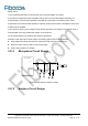
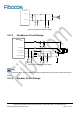
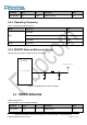
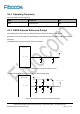
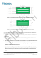
For user PCB, the characteristic impedance of all RF signal traces should be within 50ohms. In general,
the impedance of the RF signal trace is determined by the dielectric constant of the material, the trace
width (W), the ground clearance (S) and the height of the reference ground plane (H). The control of the
characteristic impedance of the PCB usually in two ways: microstrip trace and coplanar waveguide. To
illustrate the design principles, the following figures show the structural designs of microstrip trace and
coplanar waveguide when the impedance cable is at 50ohms.
⚫ Microstrip trace entirety structure
Figure 5-1 Two-layer PCB microstrip cable structure
⚫ Coplanar waveguide entirety structure
Figure 5-2 Two-layer PCB coplanar waveguide structure