
User's Manual


13-17
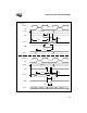
INTERFACING WITH EXTERNAL MEMORY
Following reset, the chip automatically fetches the two chip configuration bytes.
• 83C196NP only. The CCB fetches are from external memory if EA# = 0 and from internal
ROM if EA# = 1.
• 80C196NP and 80C196NU only. The CCB fetches are from external memory. (EA#
should be tied low.)
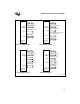
If the CCBs are stored in external ROM, chip-select output 0 (CS0#) should be connected to that
device. Chip-select output 0 is initialized for the address range FF2000–FF20FFH, which in-
cludes the CCB locations. Following the CCB fetches, the device fetches the instruction at
FF2080H.
The device uses the following bus control parameters for the CCB0 fetch:
• Bus multiplexing (DEMUX): multiplexed
• Bus width (BW16): 8 bits
• Wait states (WS0, WS1): 3 wait states. The READY pin is active for the CCB0 and CCB1
fetches and can be used to insert additional wait states (see “Wait States (Ready Control)”
on page 13-26).
CCB0 can be fetched over a 16-bit bus, even though BW16 defaults to 8 bits for the CCB0 fetch.
The upper address lines A19:8 and AD15:8 are strongly driven during the CCB0 fetch because
an 8-bit bus is assumed. Therefore, if you have a 16-bit data bus, write the value 20H to FF2019H
to avoid contention on AD15:8. Lines A19:0 are driven in the multiplexed mode. You can access
the memory using A19:0 and use AD15:0 for data only.
CCB0 itself contains bits that specify DEMUX, BW16, WS0, and WS1. These values are used to
control the CCB1 fetch, and following the fetch, they are stored in the chip-select output 0 bus
control register, BUSCON0 (see “Chip-select Unit Initial Conditions” on page 13-11). The bits
in CCB0 and CCB1 are described in “Chip Configuration Registers and Chip Configuration
Bytes” on page 13-14.