
Data Sheet

Digital interfaces LSM9DS1
36/72 DocID025715 Rev 2
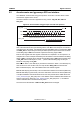
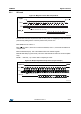
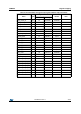
5.3.2 SPI write
Figure 25. Magnetic sensor SPI write protocol
The SPI write command is performed with 16 clock pulses. A multiple byte write command
is performed by adding blocks of 8 clock pulses to the previous one.
bit 0: WRITE bit. The value is 0.
bit 1: MS bit. When 0, does not increment the address; when 1, increments the address in
multiple writes.
bit 2 -7: address AD(5:0). This is the address field of the indexed register.
bit 8-15: data DI(7:0) (write mode). This is the data that is written inside the device (MSb
first).
bit 16-... : data DI(...-8). Further data in multiple byte writes.
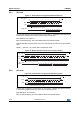
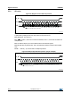
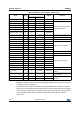
Figure 26. Multiple byte SPI write protocol (2-byte example)
CS
SPC
SDI
RW
DI7DI6DI5DI4DI3DI2DI1DI0
AD5 AD 4 AD 3 AD2 AD 1 AD0MS
AM10132V1
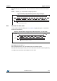
CS_M
CS
SPC
SDI
RW
AD5 AD4 AD3 AD2 AD1 AD 0
DI 7 D I6 DI 5 D I4 DI 3 DI 2 DI 1 DI 0 DI 15 D I1 4 DI 13 D I1 2 DI 11 DI 10 DI9 DI 8
MS
AM10133V1
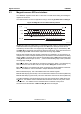
CS_M
SPC
SDI