
Application Guide


RF LAYOUT Application Guide
8 / 9
1. Control the line width W and spacing S corresponding to the 50 ohm coplanar waveguide. Take the common PCB board as FR4 medium (dielectric constant is 4.2) and the copper thickness
is 35um as an example, the line width and ground clearance corresponding to the thickness between different signal layers and reference ground are shown in Table 1. It is especially
reminded that the PCB board factory needs to control the precision of the line width W and the ground clearance S on both sides. 2. The ground PIN is not used as a thermal pad, and
should be in full contact with the ground. 3. The surface layer is slightly forbidden to reduce parasitic effects. The RF line should be as short as possible, and it is best to avoid right-angle routing.
It is recommended to go 135 degrees if there is a corner. 4. When connecting the device package, pay attention to keep the signal pins at a certain distance from the ground, please refer to
Figure 6. If it is a mounted pad, dig the ground under the corresponding signal pin pad. 5. Ensure that the reference ground corresponding to the RF line is complete, add ground holes to help
RF return, and keep at least 2 ground holes and signal lines.
Sunivision Technology Development Co.,Ltd
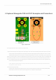
The example diagram combined with the numbers in the figure above, there are 6 points to be noted:
Pi
Figure 6: PCB LAYOUT
6. Three components make up the type
matching
circuit shown in Figure 1. When placing, the pad should be placed close to the antenna, as shown in the figure above. If the distance between the antenna connection end (SMA)
and the RF PIN pin of the module is too short to fit the three pieces of the ÿ-shaped circuit, it can be changed to an L-shaped matching circuit.
The distance to multiply the line width. Ensure that the grounding area of the same layer of the RF line is as large as possible, and the reference ground on the other side is as complete as possible, and ensure that a certain
amount of ground holes are connected to the two layers of ground.
4 Coplanar Waveguide PCB LAYOUT Examples and Precautions